HD64F2638F20J Renesas Electronics America, HD64F2638F20J Datasheet - Page 72
HD64F2638F20J
Manufacturer Part Number
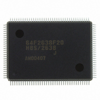
HD64F2638F20J
Description
IC H8S MCU FLASH 256K 128-QFP
Manufacturer
Renesas Electronics America
Series
H8® H8S/2600r
Specifications of HD64F2638F20J
Core Processor
H8S/2600
Core Size
16-Bit
Speed
20MHz
Connectivity
CAN, SCI, SmartCard
Peripherals
Motor Control PWM, POR, PWM, WDT
Number Of I /o
72
Program Memory Size
256KB (256K x 8)
Program Memory Type
FLASH
Ram Size
16K x 8
Voltage - Supply (vcc/vdd)
4.5 V ~ 5.5 V
Data Converters
A/D 12x10b; D/A 2x8b
Oscillator Type
Internal
Operating Temperature
-40°C ~ 85°C
Package / Case
128-QFP
Lead Free Status / RoHS Status
Contains lead / RoHS non-compliant
Eeprom Size
-
Available stocks
Company
Part Number
Manufacturer
Quantity
Price
Company:

Part Number:
HD64F2638F20J
Manufacturer:
PENESAS
Quantity:
252


Section 1 Overview
Type
I/O ports
Motor control
PWM
Notes: 1. Subclock functions (subactive mode, subsleep mode, and watch mode) are available in
Page 22 of 1458
I
(IIC) (Optionk)
(Only for the W-
mask version of
the H8S/2638,
H8S/2639, and
H8S/2630)
2
C bus interface
2. The FWE pin is functional only in the flash memory version. The FWE pin is a NC pin in
3. The HTxD1 and HRxD1 pins are not supported in H8S/2635 Group.
4. The PO15 to PO8 output are not supported in H8S/2635 Group.
5. The DA1 and DA0 output are not supported in H8S/2635 Group.
the U-mask and W-mask versions, and H8S/2635 Group.
These functions cannot be used with the other versions.
See section 22A.7, Subclock Oscillator, for the method of fixing pins OSC1 and OSC2.
The H8S/2639 and H8S/2635 Groups have no OSC1 and OSC2 pins.
the mask ROM versions. In the mask ROM version, the FWE pin must be left open or
be connected to Vss.
Symbol
PF7 to PF3,
PF0
PH7 to PH0
PJ7 to PJ0
PWM1A to
PWM1H
PWM2A to
PWM2H
PWMVCC
PWMVSS
SCL0, SCL1
SDA0, SDA1 I/O
I/O
I/O
I/O
Output
Output
Input
I/O
Input
I/O
Name and Function
Port F: A 6-bit I/O port. Input or output can be
designated for each bit by means of the port F data
direction register (PFDDR).
Port H: An 8-bit I/O port. Input or output can be
designated for each bit by means of the port B data
direction register (PHDDR).
Port J: An 8-bit I/O port. Input or output can be
designated for each bit by means of the port J data
direction register (PJDDR).
PWM output: Motor control PWM channel 1 output
pins.
PWM output: Motor control PWM channel 2 output
pins.
PWM Power Supply: Power supply pin for motor-
control PWM.
Connect to the system power supply (+5 V) when the
motor-control function is not used.
PWM Ground: Ground pin for motor-control PWM.
Connect to the system power supply (0 V).
I
input/output pins that have bus-driving capability. The
output of SCL0 is an NMOS open-drain type.
I
input/output pins that have bus-driving capability. The
output of SDA0 is an NMOS open-drain type.
2
2
C clock input/output (Channel 0/1): I
C data input/output (Channel 0/1): I
H8S/2639, H8S/2638, H8S/2636,
REJ09B0103-0800 Rev. 8.00
H8S/2630, H8S/2635 Group
2
2
C data
C clock
May 28, 2010
Related parts for HD64F2638F20J
Image
Part Number
Description
Manufacturer
Datasheet
Request
R


Part Number:
Description:
KIT STARTER FOR M16C/29
Manufacturer:
Renesas Electronics America
Datasheet:

Part Number:
Description:
KIT STARTER FOR R8C/2D
Manufacturer:
Renesas Electronics America
Datasheet:

Part Number:
Description:
R0K33062P STARTER KIT
Manufacturer:
Renesas Electronics America
Datasheet:

Part Number:
Description:
KIT STARTER FOR R8C/23 E8A
Manufacturer:
Renesas Electronics America
Datasheet:

Part Number:
Description:
KIT STARTER FOR R8C/25
Manufacturer:
Renesas Electronics America
Datasheet:

Part Number:
Description:
KIT STARTER H8S2456 SHARPE DSPLY
Manufacturer:
Renesas Electronics America
Datasheet:

Part Number:
Description:
KIT STARTER FOR R8C38C
Manufacturer:
Renesas Electronics America
Datasheet:

Part Number:
Description:
KIT STARTER FOR R8C35C
Manufacturer:
Renesas Electronics America
Datasheet:

Part Number:
Description:
KIT STARTER FOR R8CL3AC+LCD APPS
Manufacturer:
Renesas Electronics America
Datasheet:
Part Number:
Description:
KIT STARTER FOR RX610
Manufacturer:
Renesas Electronics America
Datasheet:

Part Number:
Description:
KIT STARTER FOR R32C/118
Manufacturer:
Renesas Electronics America
Datasheet:

Part Number:
Description:
KIT DEV RSK-R8C/26-29
Manufacturer:
Renesas Electronics America
Datasheet:

Part Number:
Description:
KIT STARTER FOR SH7124
Manufacturer:
Renesas Electronics America
Datasheet:

Part Number:
Description:
KIT STARTER FOR H8SX/1622
Manufacturer:
Renesas Electronics America
Datasheet: