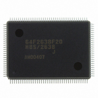
HD64F2638F20J Renesas Electronics America, HD64F2638F20J Datasheet - Page 993

HD64F2638F20J
Manufacturer Part Number
HD64F2638F20J
Description
IC H8S MCU FLASH 256K 128-QFP
Manufacturer
Renesas Electronics America
Series
H8® H8S/2600r
Specifications of HD64F2638F20J
Core Processor
H8S/2600
Core Size
16-Bit
Speed
20MHz
Connectivity
CAN, SCI, SmartCard
Peripherals
Motor Control PWM, POR, PWM, WDT
Number Of I /o
72
Program Memory Size
256KB (256K x 8)
Program Memory Type
FLASH
Ram Size
16K x 8
Voltage - Supply (vcc/vdd)
4.5 V ~ 5.5 V
Data Converters
A/D 12x10b; D/A 2x8b
Oscillator Type
Internal
Operating Temperature
-40°C ~ 85°C
Package / Case
128-QFP
Lead Free Status / RoHS Status
Contains lead / RoHS non-compliant
Eeprom Size
-
Available stocks
Company
Part Number
Manufacturer
Quantity
Price
Company:
Part Number:
HD64F2638F20J
Manufacturer:
PENESAS
Quantity:
252
- Current page: 993 of 1512
- Download datasheet (9Mb)
H8S/2639, H8S/2638, H8S/2636,
Section 23A Power-Down Modes
[HD64F2636F, HD64F2638F, HD6432636F,
H8S/2630, H8S/2635 Group
HD6432638F, HD64F2630F, HD6432630F, HD64F2635F, HD6432635F, HD6432634F]
23A.6.5 Usage Notes
I/O Port Status: In software standby mode, I/O port states are retained. If the OPE bit is set to 1,
the address bus and bus control signal output is also retained. Therefore, there is no reduction in
current dissipation for the output current when a high-level signal is output.
Current Dissipation during Oscillation Stabilization Wait Period: Current dissipation
increases during the oscillation stabilization wait period.
Write Data Buffer Function: The write data buffer function and software standby mode cannot
be used at the same time. When the write data buffer function is used, the WDBE bit in BCRL
should be cleared to 0 to cancel the write data buffer function before entering software standby
mode. Also check that external writes have finished, by reading external addresses, etc., before
executing a SLEEP instruction to enter software standby mode. See section 7.7, Write Data Buffer
Function, for details of the write data buffer function.
23A.7 Hardware Standby Mode
23A.7.1 Hardware Standby Mode
When the STBY pin is driven low, a transition is made to hardware standby mode from any mode.
In hardware standby mode, all functions enter the reset state and stop operation, resulting in a
significant reduction in power dissipation. As long as the prescribed voltage is supplied, on-chip
RAM data is retained. I/O ports are set to the high-impedance state.
In order to retain on-chip RAM data, the RAME bit in SYSCR should be cleared to 0 before
driving the STBY pin low.
Do not change the state of the mode pins (MD2 to MD0) while the chip is in hardware standby
mode.
Hardware standby mode is cleared by means of the STBY pin and the RES pin. When the STBY
pin is driven high while the RES pin is low, the reset state is set and clock oscillation is started.
Ensure that the RES pin is held low until the clock oscillator stabilizes (at least 8 ms—the
oscillation stabilization time—when using a crystal oscillator). When the RES pin is subsequently
driven high, a transition is made to the program execution state via the reset exception handling
state.
REJ09B0103-0800 Rev. 8.00
Page 943 of 1458
May 28, 2010
Related parts for HD64F2638F20J
Image
Part Number
Description
Manufacturer
Datasheet
Request
R

Part Number:
Description:
KIT STARTER FOR M16C/29
Manufacturer:
Renesas Electronics America
Datasheet:

Part Number:
Description:
KIT STARTER FOR R8C/2D
Manufacturer:
Renesas Electronics America
Datasheet:

Part Number:
Description:
R0K33062P STARTER KIT
Manufacturer:
Renesas Electronics America
Datasheet:

Part Number:
Description:
KIT STARTER FOR R8C/23 E8A
Manufacturer:
Renesas Electronics America
Datasheet:

Part Number:
Description:
KIT STARTER FOR R8C/25
Manufacturer:
Renesas Electronics America
Datasheet:

Part Number:
Description:
KIT STARTER H8S2456 SHARPE DSPLY
Manufacturer:
Renesas Electronics America
Datasheet:

Part Number:
Description:
KIT STARTER FOR R8C38C
Manufacturer:
Renesas Electronics America
Datasheet:

Part Number:
Description:
KIT STARTER FOR R8C35C
Manufacturer:
Renesas Electronics America
Datasheet:

Part Number:
Description:
KIT STARTER FOR R8CL3AC+LCD APPS
Manufacturer:
Renesas Electronics America
Datasheet:

Part Number:
Description:
KIT STARTER FOR RX610
Manufacturer:
Renesas Electronics America
Datasheet:

Part Number:
Description:
KIT STARTER FOR R32C/118
Manufacturer:
Renesas Electronics America
Datasheet:

Part Number:
Description:
KIT DEV RSK-R8C/26-29
Manufacturer:
Renesas Electronics America
Datasheet:

Part Number:
Description:
KIT STARTER FOR SH7124
Manufacturer:
Renesas Electronics America
Datasheet:

Part Number:
Description:
KIT STARTER FOR H8SX/1622
Manufacturer:
Renesas Electronics America
Datasheet:


