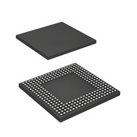
HD6417720BP133BV Renesas Electronics America, HD6417720BP133BV Datasheet - Page 427

HD6417720BP133BV
Manufacturer Part Number
HD6417720BP133BV
Description
SH3-DSP, WITH USB AND LCDC, PB-F
Manufacturer
Renesas Electronics America
Series
SuperH® SH7700r
Datasheet
1.R8A77210C133BAV.pdf
(1478 pages)
Specifications of HD6417720BP133BV
Core Processor
SH-3 DSP
Core Size
32-Bit
Speed
133MHz
Connectivity
FIFO, I²C, IrDA, MMC, SCI, SD, SIO, SIM, USB
Peripherals
DMA, LCD, POR, WDT
Number Of I /o
117
Program Memory Type
ROMless
Ram Size
16K x 8
Voltage - Supply (vcc/vdd)
1.4 V ~ 1.6 V
Data Converters
A/D 4x10b; D/A 2x8b
Oscillator Type
Internal
Operating Temperature
-20°C ~ 75°C
Package / Case
256-BGA
Lead Free Status / RoHS Status
Lead free / RoHS Compliant
Eeprom Size
-
Program Memory Size
-
- Current page: 427 of 1478
- Download datasheet (10Mb)
SH7720 Group, SH7721 Group
Section 9 Bus State Controller (BSC)
(7)
Bank Active
The SDRAM bank function is used to support high-speed accesses to the same row address. When
the BACTV bit in SDCR is 1, accesses are performed using commands without auto-precharge
(READ or WRIT). This function is called bank-active function. This function is valid only for
either the upper or lower bits of area 3. When area 3 is set to bank-active mode, area 2 should be
set to normal space or byte-selection SRAM. When areas 2 and 3 are both set to SDRAM, auto-
precharge mode must be set.
When a bank-active function is used, precharging is not performed when the access ends. When
accessing the same row address in the same bank, it is possible to issue the READ or WRIT
command immediately, without issuing an ACTV command. As SDRAM is internally divided
into several banks, it is possible to activate one row address in each bank. If the next access is to a
different row address, a PRE command is first issued to precharge the relevant bank, then when
precharging is completed, the access is performed by issuing an ACTV command followed by a
READ or WRIT command. If this is followed by an access to a different row address, the access
time will be longer because of the precharging performed after the access request is issued. The
number of cycles between issuance of the PRE command and the ACTV command is determined
by the TRP[1:0] bits in CSnWCR.
In a write, when an auto-precharge is performed, a command cannot be issued to the same bank
for a period of Trwl + Tap cycles after issuance of the WRITA command. When bank active mode
is used, READ or WRIT commands can be issued successively if the row address is the same. The
number of cycles can thus be reduced by Trwl + Tap cycles for each write.
There is a limit on tRAS, the time for placing each bank in the active state. If there is no guarantee
that there will not be a cache hit and another row address will be accessed within the period in
which this value is maintained by program execution, it is necessary to set auto-refresh and set the
refresh cycle to no more than the maximum value of tRAS.
A burst read cycle without auto-precharge is shown in figure 9.19, a burst read cycle for the same
row address in figure 9.20, and a burst read cycle for different row addresses in figure 9.21.
Similarly, a single write cycle without auto-precharge is shown in figure 9.22, a single write cycle
for the same row address in figure 9.23, and a single write cycle for different row addresses in
figure 9.24.
In figure 9.20, a Tnop cycle in which no operation is performed is inserted before the Tc cycle that
issues the READ command. The Tnop cycle is inserted to acquire two cycles of CAS latency for
the DQMxx signal that specifies the read byte in the data read from the SDRAM. If the CAS
latency is specified as two cycles or more, the Tnop cycle is not inserted because the two cycles of
latency can be acquired even if the DQMxx signal is asserted after the Tc cycle.
R01UH0083EJ0400 Rev. 4.00
Page 367 of 1414
Sep 21, 2010
Related parts for HD6417720BP133BV
Image
Part Number
Description
Manufacturer
Datasheet
Request
R

Part Number:
Description:
KIT STARTER FOR M16C/29
Manufacturer:
Renesas Electronics America
Datasheet:

Part Number:
Description:
KIT STARTER FOR R8C/2D
Manufacturer:
Renesas Electronics America
Datasheet:

Part Number:
Description:
R0K33062P STARTER KIT
Manufacturer:
Renesas Electronics America
Datasheet:

Part Number:
Description:
KIT STARTER FOR R8C/23 E8A
Manufacturer:
Renesas Electronics America
Datasheet:

Part Number:
Description:
KIT STARTER FOR R8C/25
Manufacturer:
Renesas Electronics America
Datasheet:

Part Number:
Description:
KIT STARTER H8S2456 SHARPE DSPLY
Manufacturer:
Renesas Electronics America
Datasheet:

Part Number:
Description:
KIT STARTER FOR R8C38C
Manufacturer:
Renesas Electronics America
Datasheet:

Part Number:
Description:
KIT STARTER FOR R8C35C
Manufacturer:
Renesas Electronics America
Datasheet:

Part Number:
Description:
KIT STARTER FOR R8CL3AC+LCD APPS
Manufacturer:
Renesas Electronics America
Datasheet:

Part Number:
Description:
KIT STARTER FOR RX610
Manufacturer:
Renesas Electronics America
Datasheet:

Part Number:
Description:
KIT STARTER FOR R32C/118
Manufacturer:
Renesas Electronics America
Datasheet:

Part Number:
Description:
KIT DEV RSK-R8C/26-29
Manufacturer:
Renesas Electronics America
Datasheet:

Part Number:
Description:
KIT STARTER FOR SH7124
Manufacturer:
Renesas Electronics America
Datasheet:

Part Number:
Description:
KIT STARTER FOR H8SX/1622
Manufacturer:
Renesas Electronics America
Datasheet:

Part Number:
Description:
KIT DEV FOR SH7203
Manufacturer:
Renesas Electronics America
Datasheet:


