M30835FJGP#U5 Renesas Electronics America, M30835FJGP#U5 Datasheet - Page 78
M30835FJGP#U5
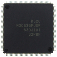
Manufacturer Part Number
M30835FJGP#U5
Description
IC M32C/83 MCU FLASH 144LQFP
Manufacturer
Renesas Electronics America
Series
M16C™ M32C/80r
Datasheets
1.M3087BFLGPU3.pdf
(364 pages)
2.M30833FJGPU3.pdf
(96 pages)
3.M30833FJGPU3.pdf
(529 pages)
Specifications of M30835FJGP#U5
Core Processor
M32C/80
Core Size
16/32-Bit
Speed
32MHz
Connectivity
CAN, I²C, IEBus, SIO, UART/USART
Peripherals
DMA, WDT
Number Of I /o
121
Program Memory Size
512KB (512K x 8)
Program Memory Type
FLASH
Ram Size
31K x 8
Voltage - Supply (vcc/vdd)
3 V ~ 5.5 V
Data Converters
A/D 34x10b, D/A 2x8b
Oscillator Type
Internal
Operating Temperature
-20°C ~ 85°C
Package / Case
144-LQFP
For Use With
R0K330879S001BE - KIT DEV RSK M32C/87R0K330879S000BE - KIT DEV RSK M32C/87
Lead Free Status / RoHS Status
Lead free / RoHS Compliant
Eeprom Size
-
Available stocks
Company
Part Number
Manufacturer
Quantity
Price

Part Number:
M30835FJGP#U5M30835FJGP#U3
Manufacturer:
Renesas Electronics America
Quantity:
10 000


R
R
M
e
E
. v
J
3
0
2
7.1.1 Selecting External Address Bus
7.1.2 Selecting External Data Bus
7.1.3 Selecting Separate/Multiplexed Bus
1
9
C
3 .
B
The number of externally-output address bus, chip-select signals and chip-select-assigned address
space (CS area) varies depending on each external space mode. The PM11 to PM10 bits in the PM1
register determine the external space mode.
When using the DRAMC, row addresses and column addresses are multiplexed to output in the DRAM
area.
The DS register selects either external 8-bit or 16-bit data bus per external space. The data bus in the
external space 3, after reset, becomes 16 bits wide when an "L" signal is applied to the BYTE pin and 8
bits wide when an "H" signal is applied. Do not change the BYTE pin level while the microcomputer is
operating. The internal bus is always 16 bits wide.
The PM05 to PM04 bits in the PM0 register determine either a separate or multiplexed bus as bus format .
8 /
0
1
7.1.3.1 Separate Bus
7.1.3.2 Multiplexed Bus
0
3
The separate bus is a bus format which allows the microcomputer to input and output data and ad-
dress using separate buses. The DS register selects 8-bit or 16-bit data bus as the external data bus
per external space. If all DSi bits in the DS register (i=0 to 3) are set to "0" (8-bit data bus), port P
becomes the data bus and port P
"1" (16-bit data bus), ports P0 and P1 become the data bus. When the microcomputer accesses a
space while the DSi bit set to "0", port P1 is indeterminate.
If the microcomputer accesses a space with the separate bus, the WCR register determines the num-
ber of software wait states inserted.
The multiplexed bus is a bus format which allows the microcomputer to input and output data and
address via bus by timesharing. D
data bus. D
microcomputer accesses a space with the multiplexed bus, the WCR register can be set to either two
wait states or three wait states. Two-wait-state access is automatically selected if the WCR register is
set to no wait state or one wait state. Refer to 7.2.4 Bus Timing for details.
The microcomputer starts operation using the separate bus after reset. Therefore, the multiplexed bus
can be assigned to access the CS1 area, the CS2 area, or all CS areas. However, the multiplexed bus
cannot be assigned to access all CS areas in microprocessor mode. When the PM05 and PM04 bits
in the PM0 register are set to "11
to A
3
J
G
4
a
0 -
n
o r
3 .
15
1
_____
u
, 1
3
, of an address are output. See Table 7.2 for details.
p
1
2
(
0
M
0
3
6
2
0
C
to D
8 /
Page 53
, 3
15
M
are multiplexed with A
3
2
C
f o
8 /
4
8
3
8
) T
_______
2
1
_____
" (access all CS areas with the bus), only 16 low-order bits, from A
0
becomes the programmable I/O port. If one of the DSi bits is set to
to D
7
are multiplexed with A
0
_______
to A
_____
15
in space accessed by the 16-bit data bus. If the
_____
0
to A
7
in space accessed by the 8-bit
7. Bus
0
0
Related parts for M30835FJGP#U5
Image
Part Number
Description
Manufacturer
Datasheet
Request
R

Part Number:
Description:
KIT STARTER FOR M16C/29
Manufacturer:
Renesas Electronics America
Datasheet:

Part Number:
Description:
KIT STARTER FOR R8C/2D
Manufacturer:
Renesas Electronics America
Datasheet:

Part Number:
Description:
R0K33062P STARTER KIT
Manufacturer:
Renesas Electronics America
Datasheet:

Part Number:
Description:
KIT STARTER FOR R8C/23 E8A
Manufacturer:
Renesas Electronics America
Datasheet:

Part Number:
Description:
KIT STARTER FOR R8C/25
Manufacturer:
Renesas Electronics America
Datasheet:

Part Number:
Description:
KIT STARTER H8S2456 SHARPE DSPLY
Manufacturer:
Renesas Electronics America
Datasheet:

Part Number:
Description:
KIT STARTER FOR R8C38C
Manufacturer:
Renesas Electronics America
Datasheet:

Part Number:
Description:
KIT STARTER FOR R8C35C
Manufacturer:
Renesas Electronics America
Datasheet:

Part Number:
Description:
KIT STARTER FOR R8CL3AC+LCD APPS
Manufacturer:
Renesas Electronics America
Datasheet:
Part Number:
Description:
KIT STARTER FOR RX610
Manufacturer:
Renesas Electronics America
Datasheet:

Part Number:
Description:
KIT STARTER FOR R32C/118
Manufacturer:
Renesas Electronics America
Datasheet:

Part Number:
Description:
KIT DEV RSK-R8C/26-29
Manufacturer:
Renesas Electronics America
Datasheet:

Part Number:
Description:
KIT STARTER FOR SH7124
Manufacturer:
Renesas Electronics America
Datasheet:

Part Number:
Description:
KIT STARTER FOR H8SX/1622
Manufacturer:
Renesas Electronics America
Datasheet:

Part Number:
Description:
KIT DEV FOR SH7203
Manufacturer:
Renesas Electronics America
Datasheet: