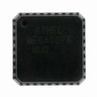
ATMEGA88PA-MU Atmel, ATMEGA88PA-MU Datasheet - Page 71

ATMEGA88PA-MU
Manufacturer Part Number
ATMEGA88PA-MU
Description
MCU AVR 8K ISP FLASH MEM 32-QFN
Manufacturer
Atmel
Series
AVR® ATmegar
Datasheets
1.ATMEGA48A-PU.pdf
(566 pages)
2.ATMEGA48A-PU.pdf
(33 pages)
3.ATMEGA48PA-MMH.pdf
(26 pages)
Specifications of ATMEGA88PA-MU
Core Processor
AVR
Core Size
8-Bit
Speed
20MHz
Connectivity
I²C, SPI, UART/USART
Peripherals
Brown-out Detect/Reset, POR, PWM, WDT
Number Of I /o
23
Program Memory Size
8KB (4K x 16)
Program Memory Type
FLASH
Eeprom Size
512 x 8
Ram Size
1K x 8
Voltage - Supply (vcc/vdd)
1.8 V ~ 5.5 V
Data Converters
A/D 8x10b
Oscillator Type
Internal
Operating Temperature
-40°C ~ 85°C
Package / Case
32-VQFN Exposed Pad, 32-HVQFN, 32-SQFN, 32-DHVQFN
Controller Family/series
AVR MEGA
No. Of I/o's
23
Eeprom Memory Size
512Byte
Ram Memory Size
1KB
Cpu Speed
20MHz
No. Of Timers
3
Rohs Compliant
Yes
Package
32QFN EP
Device Core
AVR
Family Name
ATmega
Maximum Speed
20 MHz
Operating Supply Voltage
2.5|3.3|5 V
Data Bus Width
8 Bit
Number Of Programmable I/os
23
Interface Type
SPI/TWI/USART
On-chip Adc
8-chx10-bit
Number Of Timers
3
For Use With
ATSTK600-TQFP32 - STK600 SOCKET/ADAPTER 32-TQFPATSTK600-DIP40 - STK600 SOCKET/ADAPTER 40-PDIP770-1007 - ISP 4PORT ATMEL AVR MCU SPI/JTAGATAVRDRAGON - KIT DRAGON 32KB FLASH MEM AVRATAVRISP2 - PROGRAMMER AVR IN SYSTEMATJTAGICE2 - AVR ON-CHIP D-BUG SYSTEM
Lead Free Status / RoHS Status
Lead free / RoHS Compliant
Available stocks
Company
Part Number
Manufacturer
Quantity
Price
Part Number:
ATMEGA88PA-MU
Manufacturer:
MICROCHIP/微芯
Quantity:
20 000
- Current page: 71 of 566
- Download datasheet (23Mb)
12. External Interrupts
12.1
8271C–AVR–08/10
Pin Change Interrupt Timing
The External Interrupts are triggered by the INT0 and INT1 pins or any of the PCINT23...0 pins.
Observe that, if enabled, the interrupts will trigger even if the INT0 and INT1 or PCINT23...0 pins
are configured as outputs. This feature provides a way of generating a software interrupt. The
pin change interrupt PCI2 will trigger if any enabled PCINT[23:16] pin toggles. The pin change
interrupt PCI1 will trigger if any enabled PCINT[14:8] pin toggles. The pin change interrupt PCI0
will trigger if any enabled PCINT[7:0] pin toggles. The PCMSK2, PCMSK1 and PCMSK0 Regis-
ters control which pins contribute to the pin change interrupts. Pin change interrupts on
PCINT23...0 are detected asynchronously. This implies that these interrupts can be used for
waking the part also from sleep modes other than Idle mode.
The INT0 and INT1 interrupts can be triggered by a falling or rising edge or a low level. This is
set up as indicated in the specification for the External Interrupt Control Register A – EICRA.
When the INT0 or INT1 interrupts are enabled and are configured as level triggered, the inter-
rupts will trigger as long as the pin is held low. Note that recognition of falling or rising edge
interrupts on INT0 or INT1 requires the presence of an I/O clock, described in
and their Distribution” on page
nously. This implies that this interrupt can be used for waking the part also from sleep modes
other than Idle mode. The I/O clock is halted in all sleep modes except Idle mode.
Note:
An example of timing of a pin change interrupt is shown in
Figure 12-1. Timing of pin change interrupts
ATmega48A/48PA/88A/88PA/168A/168PA/328/328
Note that if a level triggered interrupt is used for wake-up from Power-down, the required level
must be held long enough for the MCU to complete the wake-up to trigger the level interrupt. If the
level disappears before the end of the Start-up Time, the MCU will still wake up, but no interrupt
will be generated. The start-up time is defined by the SUT and CKSEL Fuses as described in
”System Clock and Clock Options” on page
pcint_setflag
pcint_in_(0)
PCINT(0)
pcint_syn
pin_sync
pin_lat
PCINT(0)
PCIF
clk
clk
LE
pin_lat
26. Low level interrupt on INT0 and INT1 is detected asynchro-
D
Q
pin_sync
PCINT(0) in PCMSK(x)
pcint_in_(0)
26.
0
x
clk
Figure
pcint_syn
12-1.
pcint_setflag
PCIF
”Clock Systems
71
Related parts for ATMEGA88PA-MU
Image
Part Number
Description
Manufacturer
Datasheet
Request
R

Part Number:
Description:
IC MCU AVR 8K 5V 20MHZ 32-TQFP
Manufacturer:
Atmel
Datasheet:

Part Number:
Description:
Manufacturer:
Atmel Corporation
Datasheet:

Part Number:
Description:
Manufacturer:
Atmel Corporation
Datasheet:

Part Number:
Description:
MCU AVR 8K FLASH 15MHZ 32-QFN
Manufacturer:
Atmel
Datasheet:

Part Number:
Description:
IC AVR MCU 8K 20MHZ 5V 32TQFP
Manufacturer:
Atmel
Datasheet:

Part Number:
Description:
IC AVR MCU 8K 20MHZ 5V 32-QFN
Manufacturer:
Atmel
Datasheet:

Part Number:
Description:
IC AVR MCU 8K 20MHZ 5V 28DIP
Manufacturer:
Atmel
Datasheet:

Part Number:
Description:
IC MCU AVR 8K 5V 20MHZ 32-TQFP
Manufacturer:
Atmel
Datasheet:

Part Number:
Description:
IC MCU AVR 8K 5V 20MHZ 32-QFN
Manufacturer:
Atmel
Datasheet:

Part Number:
Description:
IC MCU AVR 8K 5V 20MHZ 32-QFN
Manufacturer:
Atmel
Datasheet:

Part Number:
Description:
IC MCU AVR 8K 5V 20MHZ 28-DIP
Manufacturer:
Atmel
Datasheet:

Part Number:
Description:
IC MCU AVR 8K 5V 20MHZ 28-DIP
Manufacturer:
Atmel
Datasheet:

Part Number:
Description:
MCU AVR 8K FLASH 20MHZ 32TQFP
Manufacturer:
Atmel
Datasheet:


