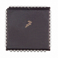
MC68HC705C8ACFN Freescale Semiconductor, MC68HC705C8ACFN Datasheet - Page 150

MC68HC705C8ACFN
Manufacturer Part Number
MC68HC705C8ACFN
Description
IC MCU 4MHZ 8K OTP 44-PLCC
Manufacturer
Freescale Semiconductor
Series
HC05r
Datasheet
1.MC68HC705C8ACFN.pdf
(222 pages)
Specifications of MC68HC705C8ACFN
Core Processor
HC05
Core Size
8-Bit
Speed
2.1MHz
Connectivity
SCI, SPI
Peripherals
POR, WDT
Number Of I /o
24
Program Memory Size
8KB (8K x 8)
Program Memory Type
OTP
Ram Size
304 x 8
Voltage - Supply (vcc/vdd)
3 V ~ 5.5 V
Oscillator Type
Internal
Operating Temperature
-40°C ~ 85°C
Package / Case
44-PLCC
Lead Free Status / RoHS Status
Contains lead / RoHS non-compliant
Eeprom Size
-
Data Converters
-
Available stocks
Company
Part Number
Manufacturer
Quantity
Price
Company:
Part Number:
MC68HC705C8ACFN
Manufacturer:
MOT
Quantity:
5 510
Company:
Part Number:
MC68HC705C8ACFN
Manufacturer:
Freescale Semiconductor
Quantity:
10 000
Part Number:
MC68HC705C8ACFN
Manufacturer:
MOTOROLA/摩托罗拉
Quantity:
20 000
Company:
Part Number:
MC68HC705C8ACFNE
Manufacturer:
Freescale Semiconductor
Quantity:
10 000
Part Number:
MC68HC705C8ACFNE
Manufacturer:
FREESCALE
Quantity:
20 000
Serial Peripheral Interface (SPI)
Technical Data
150
SPI — SPI Enable Bit
MSTR — Master Bit
CPOL — Clock Polarity Bit
CPHA — Clock Phase Bit
SPR1 and SPR0 — SPI Clock Rate Bits
This read/write bit enables the SPI. Reset clears the SPE bit.
This read/write bit selects master mode operation or slave mode
operation. Reset clears the MSTR bit.
This read/write bit determines the logic state of the PD4/SCK pin
between transmissions. To transmit data between SPIs, the SPIs
must have identical CPOL bits. Reset has no effect on the CPOL bit.
This read/write bit controls the timing relationship between the serial
clock and SPI data. To transmit data between SPIs, the SPIs must
have identical CPHA bits. When CPHA = 0, the PD5/SS pin of the
slave SPI must be set to logic 1 between bytes. Reset has no effect
on the CPHA bit.
These read/write bits select the master mode serial clock rate, as
shown in
no effect on the serial clock. Reset has no effect on SPR1 and SPR0.
Freescale Semiconductor, Inc.
For More Information On This Product,
1 = SPI enabled
0 = SPI disabled
1 = Master mode
0 = Slave mode
1 = PD4/SCK pin at logic 1 between transmissions
0 = PD4/SCK pin at logic 0 between transmissions
1 = Edge following first active edge on PD4/SCK latches data
0 = First active edge on PD4/SCK latches data
Serial Peripheral Interface (SPI)
Table
Go to: www.freescale.com
Table 11-1. SPI Clock Rate Selection
SPR[1:0]
11-1. The SPR1 and SPR0 bits of a slave SPI have
00
01
10
11
Internal Clock
Internal Clock
Internal Clock
Internal Clock
SPI Clock Rate
MC68HC705C8A — Rev. 3
32
16
2
4
MOTOROLA


