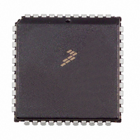
MC68HC705C9ACFN Freescale Semiconductor, MC68HC705C9ACFN Datasheet - Page 103

MC68HC705C9ACFN
Manufacturer Part Number
MC68HC705C9ACFN
Description
IC MCU 2.1MHZ 16K OTP 44-PLCC
Manufacturer
Freescale Semiconductor
Series
HC05r
Datasheet
1.MC705C9ACPE.pdf
(118 pages)
Specifications of MC68HC705C9ACFN
Core Processor
HC05
Core Size
8-Bit
Speed
2.1MHz
Connectivity
SCI, SPI
Peripherals
POR, WDT
Number Of I /o
24
Program Memory Size
16KB (16K x 8)
Program Memory Type
OTP
Ram Size
352 x 8
Voltage - Supply (vcc/vdd)
3 V ~ 5.5 V
Oscillator Type
Internal
Operating Temperature
-40°C ~ 85°C
Package / Case
44-PLCC
Lead Free Status / RoHS Status
Contains lead / RoHS non-compliant
Eeprom Size
-
Data Converters
-
Available stocks
Company
Part Number
Manufacturer
Quantity
Price
Company:
Part Number:
MC68HC705C9ACFN
Manufacturer:
Freescale Semiconductor
Quantity:
10 000
Company:
Part Number:
MC68HC705C9ACFNE
Manufacturer:
RFMD
Quantity:
8 729
Company:
Part Number:
MC68HC705C9ACFNE
Manufacturer:
Freescale Semiconductor
Quantity:
10 000
12.10 3.3- Vdc Serial Peirpheral Interface Timing
Freescale Semiconductor
1. V
2. Signal production depends on software.
3. Assumes 200 pF load on all SPI pins.
No.
10
11
12
13
1
2
3
4
5
6
7
8
9
DD
= 3.3 Vdc ± 0.3 Vdc; V
Operating frequency
Cycle time
Enable lead time
Enable lag time
Clock (SCK) high time
Clock (SCK) low time
Data setup time (inputs)
Data hold time (inputs)
Slave access time (time to data active from
high-impedance state)
Slave disable time (hold time to high-impedance state)
Data valid
Data hold time (outputs)
Rise time (20% V
Fall time (70% V
Master
Slave
Master
Slave
Master
Slave
Master
Slave
Master
Slave
Master
Slave
Master
Slave
Master
Slave
Master (before capture edge)
Slave (after enable edge)
Master (after capture edge)
Slave (after enable edge)
SPI outputs (SCK, MOSI, and MISO)
SPI inputs (SCK, MOSI, MISO, and SS)
SPI outputs (SCK, MOSI, and MISO)
SPI inputs (SCK, MOSI, MISO, and SS)
DD
DD
to 20% V
to 70% V
SS
MC68HC05C9A Advance Information Data Sheet, Rev. 4.1
= 0 Vdc, T
Characteristic
(3)
DD
DD
, C
, C
L
A
L
= 200 pF)
= –40 to +85 °C, unless otherwise noted. Refer to
= 200 pF)
(1)
t
Symbol
t
t
t
W
t
W
W
t
W
t
t
t
t
LEAD
LEAD
3.3- Vdc Serial Peirpheral Interface Timing
f
t
t
f
CYC
t
t
CYC
LAG
LAG
(
(
(
OP
(
t
t
t
HO
OP
SU
SU
t
HO
SCKH
SCKH
SCKL
t
SCKL
H
V
t
t
t
H
V
t
DIS
t
RM
FM
RS
FS
(
(
(
(
A
(
(
(
(
M
M
S
(
(
S
(
M
(
(
(
M
S
S
M
S
(
(
M
M
S
S
)
)
)
)
M
S
)
)
)
)
)
)
)
)
)
)
)
)
)
)
)
)
M
M
S
S
Figure 12-9
0.25
0.25
Min
500
720
400
720
400
200
200
200
200
2.0
1.0
1.5
dc
dc
(2)
(2)
—
—
—
—
—
—
0
0
and
Max
250
500
500
200
200
0.5
1.0
2.0
2.0
—
—
—
—
—
—
—
—
—
—
—
—
—
—
—
—
—
Figure
t
t
MHz
CYC
CYC
12-10.
Unit
t
f
CYC
µs
ns
ns
µs
ns
ns
ns
ns
ns
ns
ns
ns
ns
µs
ns
µs
OP
(
(
M
M
103
)
)


