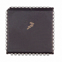
MC68HC705C9ACFN Freescale Semiconductor, MC68HC705C9ACFN Datasheet - Page 15

MC68HC705C9ACFN
Manufacturer Part Number
MC68HC705C9ACFN
Description
IC MCU 2.1MHZ 16K OTP 44-PLCC
Manufacturer
Freescale Semiconductor
Series
HC05r
Datasheet
1.MC705C9ACPE.pdf
(118 pages)
Specifications of MC68HC705C9ACFN
Core Processor
HC05
Core Size
8-Bit
Speed
2.1MHz
Connectivity
SCI, SPI
Peripherals
POR, WDT
Number Of I /o
24
Program Memory Size
16KB (16K x 8)
Program Memory Type
OTP
Ram Size
352 x 8
Voltage - Supply (vcc/vdd)
3 V ~ 5.5 V
Oscillator Type
Internal
Operating Temperature
-40°C ~ 85°C
Package / Case
44-PLCC
Lead Free Status / RoHS Status
Contains lead / RoHS non-compliant
Eeprom Size
-
Data Converters
-
Available stocks
Company
Part Number
Manufacturer
Quantity
Price
Company:
Part Number:
MC68HC705C9ACFN
Manufacturer:
Freescale Semiconductor
Quantity:
10 000
Company:
Part Number:
MC68HC705C9ACFNE
Manufacturer:
RFMD
Quantity:
8 729
Company:
Part Number:
MC68HC705C9ACFNE
Manufacturer:
Freescale Semiconductor
Quantity:
10 000
1.3 Configuration Options
The options and functions of the MC68HC705C9A can be configured to emulate either the
MC68HC05C9A or the MC68HC05C12A.
The ROM device MC68HC05C9A has eight ROM mask options to select external interrupt/internal pullup
capability on each of the eight port B bits. Other optional features are controlled by software addressable
registers during operation of the microcontroller. These features are IRQ sensitivity and memory map
configuration.
On the ROM device MC68HC05C12A, all optional features are controlled by ROM mask options. These
features are the eight port B interrupt/pullup options, IRQ sensitivity, STOP instruction disable, and COP
enable.
On the MC68HC705C9A the ROM mask options of the MC68HC05C9A and the MC68HC05C12A are
controlled by mask option registers (MORs). The MORs are EPROM registers which must be
programmed appropriately prior to operation of the microcontroller. The software options of the
MC68HC05C9A are implemented by identical software registers in the MC68HC705C9A.
When configured as an MC68HC05C9A:
When configured as an MC68HC05C12A:
Freescale Semiconductor
•
•
•
•
•
•
•
•
•
•
•
•
•
•
The entire 16K memory map of the C9A is enabled, including dual-mapped RAM and EPROM at
locations $0020–$004F and $0100–$017F.
C12A options in the C12MOR ($3FF1) are disabled.
The C9A option register ($3FDF) is enabled, allowing software control over the IRQ sensitivity and
the memory map configuration.
The C9A COP reset register ($001D) and the C9A COP control register ($001E) are enabled,
allowing software control over the C9A COP and clock monitor.
The C12 COP clear register ($3FF0) is disabled.
The port D data direction register ($0007) is enabled, allowing output capability on the seven port
D pins.
SPI output signals (MOSI, MISO, and SCK) require the corresponding bits in the port D data
direction register to be set for output.
The port D wire-OR mode control bit (bit 5 of SPCR $000A) is enabled, allowing open-drain
configuration of port D.
The RESET pin becomes bidirectional; this pin is driven low by a C9A COP or clock monitor
timeout or during power-on reset.
Memory locations $0100–$0FFF are disabled, creating a memory map identical to the
MC68HC05C12A.
C12A options in the C12MOR ($3FF1) are enabled; these bits control IRQ sensitivity, STOP
instruction disable and C12 COP enable.
The C9A option register ($3FDF) is disabled, preventing software control over the IRQ sensitivity
and the memory map configuration.
The C9A COP reset register ($001D) and the C9A COP control register ($001E) are disabled,
preventing software control over the C9A COP and clock monitor.
The C12 COP clear register ($3FF0) is enabled; this write-only register is used to clear the C12
COP.
MC68HC05C9A Advance Information Data Sheet, Rev. 4.1
Configuration Options
15


