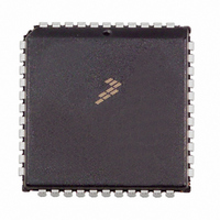
MC68HC705C9ACFN Freescale Semiconductor, MC68HC705C9ACFN Datasheet - Page 23

MC68HC705C9ACFN
Manufacturer Part Number
MC68HC705C9ACFN
Description
IC MCU 2.1MHZ 16K OTP 44-PLCC
Manufacturer
Freescale Semiconductor
Series
HC05r
Datasheet
1.MC705C9ACPE.pdf
(118 pages)
Specifications of MC68HC705C9ACFN
Core Processor
HC05
Core Size
8-Bit
Speed
2.1MHz
Connectivity
SCI, SPI
Peripherals
POR, WDT
Number Of I /o
24
Program Memory Size
16KB (16K x 8)
Program Memory Type
OTP
Ram Size
352 x 8
Voltage - Supply (vcc/vdd)
3 V ~ 5.5 V
Oscillator Type
Internal
Operating Temperature
-40°C ~ 85°C
Package / Case
44-PLCC
Lead Free Status / RoHS Status
Contains lead / RoHS non-compliant
Eeprom Size
-
Data Converters
-
Available stocks
Company
Part Number
Manufacturer
Quantity
Price
Company:
Part Number:
MC68HC705C9ACFN
Manufacturer:
Freescale Semiconductor
Quantity:
10 000
Company:
Part Number:
MC68HC705C9ACFNE
Manufacturer:
RFMD
Quantity:
8 729
Company:
Part Number:
MC68HC705C9ACFNE
Manufacturer:
Freescale Semiconductor
Quantity:
10 000
Functional Pin Descriptions
1.6.5 RESET
As an input pin, this active low RESET pin is used to reset the MCU to a known startup state by pulling
RESET low. As an output pin, when in MC68HC05C9A mode only, the RESET pin indicates that an
internal MCU reset has occurred. The RESET pin contains an internal Schmitt trigger as part of its input
to improve noise immunity. Refer to
Chapter 5 Resets
for more detail.
1.6.6 TCAP
This pin controls the input capture feature for the on-chip programmable timer. The TCAP pin contains an
internal Schmitt trigger as part of its input to improve noise immunity. Refer to
Chapter 8
Capture/Compare Timer
for more detail.
1.6.7 TCMP
The TCMP pin provides an output for the output compare feature of the on-chip programmable timer.
Refer to
Chapter 8 Capture/Compare Timer
for more detail.
1.6.8 PA0–PA7
These eight I/O lines comprise port A. The state of each pin is software programmable and all port A pins
are configured as inputs during reset. Refer to
Chapter 7 Input/Output (I/O) Ports
for more detail.
1.6.9 PB0–PB7
These eight I/O lines comprise port B. The state of each pin is software programmable and all port B pins
are configured as inputs during reset. Port B has mask option register enabled pullup devices and
interrupt capability selectable for any pin. Refer to
Chapter 7 Input/Output (I/O) Ports
for more detail.
1.6.10 PC0–PC7
These eight I/O lines comprise port C. The state of each pin is software programmable and all port C pins
are configured as inputs during reset. PC7 has high current sink and source capability. Refer to
Chapter 7 Input/Output (I/O) Ports
for more detail.
1.6.11 PD0–PD5 and PD7
These seven I/O lines comprise port D. When configured as a C9A the state of each pin is software
programmable and all port D pins are configured as inputs during reset. When configured as a C12A, the
port D pins are input only. Refer to
Chapter 7 Input/Output (I/O) Ports
for more detail.
MC68HC05C9A Advance Information Data Sheet, Rev. 4.1
Freescale Semiconductor
23


