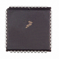
MC68HC705C9ACFN Freescale Semiconductor, MC68HC705C9ACFN Datasheet - Page 65

MC68HC705C9ACFN
Manufacturer Part Number
MC68HC705C9ACFN
Description
IC MCU 2.1MHZ 16K OTP 44-PLCC
Manufacturer
Freescale Semiconductor
Series
HC05r
Datasheet
1.MC705C9ACPE.pdf
(118 pages)
Specifications of MC68HC705C9ACFN
Core Processor
HC05
Core Size
8-Bit
Speed
2.1MHz
Connectivity
SCI, SPI
Peripherals
POR, WDT
Number Of I /o
24
Program Memory Size
16KB (16K x 8)
Program Memory Type
OTP
Ram Size
352 x 8
Voltage - Supply (vcc/vdd)
3 V ~ 5.5 V
Oscillator Type
Internal
Operating Temperature
-40°C ~ 85°C
Package / Case
44-PLCC
Lead Free Status / RoHS Status
Contains lead / RoHS non-compliant
Eeprom Size
-
Data Converters
-
Available stocks
Company
Part Number
Manufacturer
Quantity
Price
Company:
Part Number:
MC68HC705C9ACFN
Manufacturer:
Freescale Semiconductor
Quantity:
10 000
Company:
Part Number:
MC68HC705C9ACFNE
Manufacturer:
RFMD
Quantity:
8 729
Company:
Part Number:
MC68HC705C9ACFNE
Manufacturer:
Freescale Semiconductor
Quantity:
10 000
9.12 Transmit Data Out (TDO)
Transmit data is the serial data from the internal data bus that is applied through the SCI to the output
line. Data format is as discussed in
a bit time by using a derivative of the RT clock, thus producing a transmission rate equal to 1/16th that of
the receiver sample clock.
9.13 SCI I/O Registers
The following I/O registers control and monitor SCI operation:
9.13.1 SCI Data Register
The SCI data register (SCDR), shown in
characters transmitted.
9.13.2 SCI Control Register 1
The SCI control register 1 (SCCR1), shown in
R8 — Bit 8 (Received)
Freescale Semiconductor
•
•
•
•
•
•
•
When the SCI is receiving 9-bit characters, R8 is the ninth bit of the received character. R8 receives
the ninth bit at the same time that the SCDR receives the other eight bits. Resets have no effect on the
R8 bit.
SCI data register (SCDR)
SCI control register 1 (SCCR1)
SCI control register 2 (SCCR2)
SCI status register (SCSR)
Stores ninth SCI data bit received and ninth SCI data bit transmitted
Controls SCI character length
Controls SCI wakeup method
Reset:
$000E
Reset:
$0011
Read:
Read:
Write:
Write:
BIT7
Bit 7
Bit 7
R8
U
MC68HC05C9A Advance Information Data Sheet, Rev. 4.1
Figure 9-9. SCI Control Register 1 (SCCR1)
= Unimplemented
Figure 9-8. SCI Data Register (SCDR)
BIT6
T8
U
6
6
9.6 Data Format
Figure
BIT55
5
5
0
Figure
9-8, is the buffer for characters received and for
U = Undetermined
Unaffected by reset
BIT4
M
U
4
4
and shown in
9-9, has these functions:
WAKE
BIT3
U
3
3
Figure
BIT2
2
2
0
9-3. The transmitter generates
BIT1
1
1
0
Transmit Data Out (TDO)
Bit 0
BIT0
Bit 0
0
65


