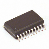
MC68HC705J1ACDW Freescale Semiconductor, MC68HC705J1ACDW Datasheet - Page 122

MC68HC705J1ACDW
Manufacturer Part Number
MC68HC705J1ACDW
Description
IC MCU 4MHZ 1.2K OTP 20-SOIC
Manufacturer
Freescale Semiconductor
Series
HC05r
Datasheet
1.MCHRC705J1ACDWE.pdf
(162 pages)
Specifications of MC68HC705J1ACDW
Core Processor
HC05
Core Size
8-Bit
Speed
4MHz
Peripherals
POR, WDT
Number Of I /o
14
Program Memory Size
1.2KB (1.2K x 8)
Program Memory Type
OTP
Ram Size
64 x 8
Voltage - Supply (vcc/vdd)
3 V ~ 5.5 V
Oscillator Type
Internal
Operating Temperature
-40°C ~ 85°C
Package / Case
20-SOIC (7.5mm Width)
Lead Free Status / RoHS Status
Contains lead / RoHS non-compliant
Eeprom Size
-
Data Converters
-
Connectivity
-
Available stocks
Company
Part Number
Manufacturer
Quantity
Price
Part Number:
MC68HC705J1ACDW
Manufacturer:
MOTOROLA/摩托罗拉
Quantity:
20 000
Company:
Part Number:
MC68HC705J1ACDWE
Manufacturer:
INTERSIL
Quantity:
1 000
Electrical Specifications
10.8 3.3-Volt DC Electrical Characteristics
Technical Data
Output voltage
Output high voltage
Output low voltage
Input high voltage
Input low voltage
Supply current
I/O ports hi-z leakage current
Input pulldown current
Input pullup current
Input current
Capacitance
Crystal/ceramic resonator oscillator mode internal resistor
1. V
2. Typical values at midpoint of voltage range, 25 C only
3. Run mode I
4. Wait mode I
5. Stop mode I
6. Only input high current rated to +1 A on RESET.
7. The R
I
I
(I
(I
(I
PA0–PA7, PB0–PB5, IRQ/V
PA0–PA7, PB0–PB5, IRQ/V
Run Mode
Wait Mode
Stop Mode
PA0–PA7, PB0–PB5 (without individual pulldown activated)
PA0–PA7, PB0–PB5 (with individual pulldown activated)
RESET
RESET, IRQ/V
Ports (as inputs or outputs)
RESET, IRQ/V
OSC1 to OSC2
Load
Load
less than 50 pF on all outputs; C
with all ports configured as inputs; V
clock source (f
V
additional information.
Load
Load
Load
DD
IH
25 C
–40 to 105 C
= V
= 3.3 Vdc
= 10.0 A
= –10.0 A
= –0.2 mA) PA0–PA7, PB0–PB5
= 0.4 mA) PA0–PA3, PB0–PB5
= 5.0 mA) PA4–PA7
osc
DD
value selected for RC oscillator versions of this device is unspecified. See
(6)
(3)
– 0.2 V
(4)
(5)
DD
DD
DD
is measured using external square wave clock source (f
osc
: only timer system active. Wait mode is affected linearly by OSC2 capacitance. Wait mode is measured
is measured with OSC1 = V
PP
PP
(7)
10%, V
, OSC1, OSC2
, OSC1
= 2.0 MHz); all inputs 0.2 V from rail; no dc loads; less than 50 pF on all outputs; C
Characteristic
SS
= 0 Vdc, T
PP
PP
Freescale Semiconductor, Inc.
L
, RESET, OSC1
, RESET, OSC1
For More Information On This Product,
= 20 pF on OSC2
IL
(1)
A
= 0.2 V; V
= –40 C to +105 C, unless otherwise noted
SS
Go to: www.freescale.com
. Stop mode I
Electrical Specifications
IH
= V
DD
– 0.2 V. Wait mode I
DD
is measured with all ports configured as inputs; V
Symbol
C
R
V
V
V
V
V
V
I
C
I
I
I
I
DD
osc
OH
OH
Out
osc
OL
OL
IL
IL
IL
In
IH
IL
In
= 2.0 MHz); all inputs 0.2 V from rail; no dc loads;
V
0.7
DD
V
DD
DD
V
is measured using external square wave
Min
–10
1.0
12
—
—
—
—
—
—
—
—
—
—
– 0.1
SS
– 0.3
V
Appendix C. MC68HSR705J1A
DD
MC68HC705J1A — Rev. 4.0
Typ
0.25
–25
1.2
0.1
1.0
0.1
0.1
2.0
30
—
—
—
—
—
—
—
—
(2)
L
= 20 pF on OSC2.
0.2
Max
V
100
–45
0.1
0.3
0.3
4.0
1.5
3.0
10
12
—
—
DD
5
8
1
1
V
DD
IL
= 0.2 V;
Unit
M
mA
mA
pF
V
V
V
V
V
for
A
A
A
A
A
A


