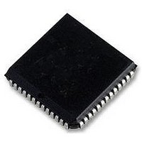
MC68HC11E0CFNE3 Freescale Semiconductor, MC68HC11E0CFNE3 Datasheet - Page 15

MC68HC11E0CFNE3
Manufacturer Part Number
MC68HC11E0CFNE3
Description
IC MCU 8BIT 3MHZ 52-PLCC
Manufacturer
Freescale Semiconductor
Series
HC11r
Specifications of MC68HC11E0CFNE3
Core Processor
HC11
Core Size
8-Bit
Speed
3MHz
Connectivity
SCI, SPI
Peripherals
POR, WDT
Number Of I /o
38
Program Memory Type
ROMless
Ram Size
512 x 8
Voltage - Supply (vcc/vdd)
4.5 V ~ 5.5 V
Data Converters
A/D 8x8b
Oscillator Type
Internal
Operating Temperature
-40°C ~ 85°C
Package / Case
52-PLCC
Controller Family/series
68HC11
No. Of I/o's
38
Ram Memory Size
512Byte
Cpu Speed
3MHz
No. Of Timers
1
Embedded Interface Type
SCI, SPI
Digital Ic Case Style
LCC
Rohs Compliant
Yes
Processor Series
HC11E
Core
HC11
Data Bus Width
8 bit
Data Ram Size
512 B
Interface Type
SCI, SPI
Maximum Clock Frequency
3 MHz
Number Of Programmable I/os
38
Number Of Timers
8
Maximum Operating Temperature
+ 85 C
Mounting Style
SMD/SMT
Minimum Operating Temperature
- 40 C
On-chip Adc
8 bit, 8 Channel
Lead Free Status / RoHS Status
Lead free / RoHS Compliant
Eeprom Size
-
Program Memory Size
-
Lead Free Status / Rohs Status
Details
Available stocks
Company
Part Number
Manufacturer
Quantity
Price
Company:
Part Number:
MC68HC11E0CFNE3
Manufacturer:
FREESCALE
Quantity:
6 249
Company:
Part Number:
MC68HC11E0CFNE3
Manufacturer:
Freescale Semiconductor
Quantity:
10 000
Company:
Part Number:
MC68HC11E0CFNE3R
Manufacturer:
Freescale Semiconductor
Quantity:
10 000
2.3 Crystal Driver and External Clock Input (XTAL, EXTAL)
TECHNICAL DATA
constant can cause the device to misinterpret the type of reset that occurred. Refer to
SECTION 5 RESETS AND INTERRUPTS for further information.
Figure 2-3 illustrates a reset circuit that uses an external switch. Use a low voltage
interrupt circuit, however, to prevent corruption of RAM.
These two pins provide the interface for either a crystal or a CMOS compatible clock
to control the internal clock generator circuitry. The frequency applied to these pins is
four times higher than the desired E-clock rate.
The XTAL pin is normally left unterminated when an external CMOS compatible clock
input is connected to the EXTAL pin. However, a 10 k
nected from XTAL to ground can be used to reduce RFI noise emission. The XTAL
output is normally intended to drive only a crystal. The XTAL output can be buffered
with a high impedance buffer, or it can be used to drive the EXTAL input of another
M68HC11.
In all cases, use caution around the oscillator pins. Load capacitances shown in the
oscillator circuits include all stray layout capacitances. Refer to Figure 2-4, Figure 2-
5, and Figure 2-6.
*
THIS VALUE INCLUDES ALL STRAY CAPACITANCES.
MC34(0/1)64
MCU
Figure 2-4 Common Crystal Connections
GND
EXTAL
V DD
IN
Freescale Semiconductor, Inc.
XTAL
RESET
2
3
For More Information On This Product,
Figure 2-3 External Reset Circuit
1
Go to: www.freescale.com
V DD
PIN DESCRIPTIONS
4.7 k
10 M
TO RESET
OF M68HC11
CRYSTAL
4 x E
25 pF
25 pF
to 100 k
EXT RESET CIRCUIT
*
*
load resistor con-
COMMON XTAL CONN
2-3


