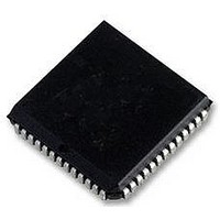
MC68HC11E0CFNE3 Freescale Semiconductor, MC68HC11E0CFNE3 Datasheet - Page 17

MC68HC11E0CFNE3
Manufacturer Part Number
MC68HC11E0CFNE3
Description
IC MCU 8BIT 3MHZ 52-PLCC
Manufacturer
Freescale Semiconductor
Series
HC11r
Specifications of MC68HC11E0CFNE3
Core Processor
HC11
Core Size
8-Bit
Speed
3MHz
Connectivity
SCI, SPI
Peripherals
POR, WDT
Number Of I /o
38
Program Memory Type
ROMless
Ram Size
512 x 8
Voltage - Supply (vcc/vdd)
4.5 V ~ 5.5 V
Data Converters
A/D 8x8b
Oscillator Type
Internal
Operating Temperature
-40°C ~ 85°C
Package / Case
52-PLCC
Controller Family/series
68HC11
No. Of I/o's
38
Ram Memory Size
512Byte
Cpu Speed
3MHz
No. Of Timers
1
Embedded Interface Type
SCI, SPI
Digital Ic Case Style
LCC
Rohs Compliant
Yes
Processor Series
HC11E
Core
HC11
Data Bus Width
8 bit
Data Ram Size
512 B
Interface Type
SCI, SPI
Maximum Clock Frequency
3 MHz
Number Of Programmable I/os
38
Number Of Timers
8
Maximum Operating Temperature
+ 85 C
Mounting Style
SMD/SMT
Minimum Operating Temperature
- 40 C
On-chip Adc
8 bit, 8 Channel
Lead Free Status / RoHS Status
Lead free / RoHS Compliant
Eeprom Size
-
Program Memory Size
-
Lead Free Status / Rohs Status
Details
Available stocks
Company
Part Number
Manufacturer
Quantity
Price
Company:
Part Number:
MC68HC11E0CFNE3
Manufacturer:
FREESCALE
Quantity:
6 249
Company:
Part Number:
MC68HC11E0CFNE3
Manufacturer:
Freescale Semiconductor
Quantity:
10 000
Company:
Part Number:
MC68HC11E0CFNE3R
Manufacturer:
Freescale Semiconductor
Quantity:
10 000
2.7 MODA and MODB (MODA/LIR,and MODB/V
2.8 PD6/AS
2.9 PD7/R/W
TECHNICAL DATA
sensitive, it can be connected to a multiple-source wired-OR network with an external
pullup resistor to V
Whenever XIRQ or IRQ are used with multiple interrupt sources (IRQ must be config-
ured for level-sensitive operation if there is more than one source of IRQ interrupt),
each source must drive the interrupt input with an open-drain type of driver to avoid
contention between outputs. There should be a single pullup resistor near the MCU
interrupt input pin (typically 4.7 k ). There must also be an interlock mechanism at
each interrupt source so that the source holds the interrupt line low until the MCU rec-
ognizes and acknowledges the interrupt request. If one or more interrupt sources are
still pending after the MCU services a request, the interrupt line will still be held low
and the MCU will be interrupted again as soon as the interrupt mask bit in the MCU is
cleared (normally upon return from an interrupt). Refer to SECTION 5 RESETS AND
INTERRUPTS.
During reset, MODA and MODB select one of the four operating modes. Refer to SEC-
TION 4 OPERATING MODES AND ON-CHIP MEMORY.
After the operating mode has been selected, the LIR pin provides an open-drain output
to indicate that execution of an instruction has begun. A series of E-clock cycles occurs
during execution of each instruction. The LIR signal goes low during the first E-clock
cycle of each instruction (opcode fetch). This output is provided for assistance in pro-
gram debugging.
The V
more than one MOS threshold (about 0.7 volts) above the V
192-byte RAM and part of the reset logic are powered from this signal rather than the
V
MCU. Reset must be driven low before V
has been restored to a valid level.
This pin performs either of two separate functions, depending on the operating mode.
In single-chip and bootstrap modes, the pin functions as input/output port D bit 6. In
the expanded multiplexed and test modes, it provides an address strobe (AS) function.
The AS can demultiplex the address and data signals at port C. Refer to SECTION 4
OPERATING MODES AND ON-CHIP MEMORY for further information.
This pin provides two separate functions, depending on the operating mode. In single-
chip and bootstrap modes, PD7/R/W acts as input/output port D bit 7. Refer to SEC-
TION 6 PARALLEL I/O for further information.
In expanded multiplexed and test modes, PD7/R/W performs a read/write function.
PD7/R/W controls the direction of transfers on the external data bus. A high on this pin
indicates that a read cycle is in progress.
DD
input. This allows RAM contents to be retained without V
STBY
pin is used to input RAM standby power. When the voltage on this pin is
DD
Freescale Semiconductor, Inc.
. XIRQ is often used as a power loss detect interrupt.
For More Information On This Product,
Go to: www.freescale.com
PIN DESCRIPTIONS
DD
is removed and must remain low until V
STBY
)
DD
DD
power applied to the
voltage, the internal
DD
2-5


