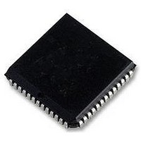
MC68HC11E0CFNE3 Freescale Semiconductor, MC68HC11E0CFNE3 Datasheet - Page 79

MC68HC11E0CFNE3
Manufacturer Part Number
MC68HC11E0CFNE3
Description
IC MCU 8BIT 3MHZ 52-PLCC
Manufacturer
Freescale Semiconductor
Series
HC11r
Specifications of MC68HC11E0CFNE3
Core Processor
HC11
Core Size
8-Bit
Speed
3MHz
Connectivity
SCI, SPI
Peripherals
POR, WDT
Number Of I /o
38
Program Memory Type
ROMless
Ram Size
512 x 8
Voltage - Supply (vcc/vdd)
4.5 V ~ 5.5 V
Data Converters
A/D 8x8b
Oscillator Type
Internal
Operating Temperature
-40°C ~ 85°C
Package / Case
52-PLCC
Controller Family/series
68HC11
No. Of I/o's
38
Ram Memory Size
512Byte
Cpu Speed
3MHz
No. Of Timers
1
Embedded Interface Type
SCI, SPI
Digital Ic Case Style
LCC
Rohs Compliant
Yes
Processor Series
HC11E
Core
HC11
Data Bus Width
8 bit
Data Ram Size
512 B
Interface Type
SCI, SPI
Maximum Clock Frequency
3 MHz
Number Of Programmable I/os
38
Number Of Timers
8
Maximum Operating Temperature
+ 85 C
Mounting Style
SMD/SMT
Minimum Operating Temperature
- 40 C
On-chip Adc
8 bit, 8 Channel
Lead Free Status / RoHS Status
Lead free / RoHS Compliant
Eeprom Size
-
Program Memory Size
-
Lead Free Status / Rohs Status
Details
Available stocks
Company
Part Number
Manufacturer
Quantity
Price
Company:
Part Number:
MC68HC11E0CFNE3
Manufacturer:
FREESCALE
Quantity:
6 249
Company:
Part Number:
MC68HC11E0CFNE3
Manufacturer:
Freescale Semiconductor
Quantity:
10 000
Company:
Part Number:
MC68HC11E0CFNE3R
Manufacturer:
Freescale Semiconductor
Quantity:
10 000
8.1 Functional Description
TECHNICAL DATA
The serial peripheral interface (SPI), an independent serial communications sub-
system, allows the MCU to communicate synchronously with peripheral devices, such
as transistor-transistor logic (TTL) shift registers, liquid crystal diode (LCD) display
drivers, analog-to-digital converter subsystems, and other microprocessors. The SPI
is also capable of inter-processor communication in a multiple master system. The SPI
system can be configured as either a master or a slave device with data rates as high
as one half of the E-clock rate when configured as master, and as fast as the E-clock
rate when configured as slave.
The central element in the SPI system is the block containing the shift register and the
read data buffer. The system is single buffered in the transmit direction and double
buffered in the receive direction. This means that new data for transmission cannot be
written to the shifter until the previous transfer is complete; however, received data is
transferred into a parallel read data buffer so the shifter is free to accept a second se-
rial character. As long as the first character is read out of the read data buffer before
the next serial character is ready to be transferred, no overrun condition occurs. A sin-
gle MCU register address is used for reading data from the read data buffer, and for
writing data to the shifter.
The SPI status block represents the SPI status functions (transfer complete, write col-
lision, and mode fault) performed by the serial peripheral status register (SPSR). The
SPI control block represents those functions that control the SPI system through the
serial peripheral control register (SPCR).
Refer to Figure 8-1, which shows the SPI block diagram.
SERIAL PERIPHERAL INTERFACE
Freescale Semiconductor, Inc.
For More Information On This Product,
SERIAL PERIPHERAL INTERFACE
Go to: www.freescale.com
SECTION 8
8-1


