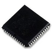
MC68HC11E0CFNE3 Freescale Semiconductor, MC68HC11E0CFNE3 Datasheet - Page 91

MC68HC11E0CFNE3
Manufacturer Part Number
MC68HC11E0CFNE3
Description
IC MCU 8BIT 3MHZ 52-PLCC
Manufacturer
Freescale Semiconductor
Series
HC11r
Specifications of MC68HC11E0CFNE3
Core Processor
HC11
Core Size
8-Bit
Speed
3MHz
Connectivity
SCI, SPI
Peripherals
POR, WDT
Number Of I /o
38
Program Memory Type
ROMless
Ram Size
512 x 8
Voltage - Supply (vcc/vdd)
4.5 V ~ 5.5 V
Data Converters
A/D 8x8b
Oscillator Type
Internal
Operating Temperature
-40°C ~ 85°C
Package / Case
52-PLCC
Controller Family/series
68HC11
No. Of I/o's
38
Ram Memory Size
512Byte
Cpu Speed
3MHz
No. Of Timers
1
Embedded Interface Type
SCI, SPI
Digital Ic Case Style
LCC
Rohs Compliant
Yes
Processor Series
HC11E
Core
HC11
Data Bus Width
8 bit
Data Ram Size
512 B
Interface Type
SCI, SPI
Maximum Clock Frequency
3 MHz
Number Of Programmable I/os
38
Number Of Timers
8
Maximum Operating Temperature
+ 85 C
Mounting Style
SMD/SMT
Minimum Operating Temperature
- 40 C
On-chip Adc
8 bit, 8 Channel
Lead Free Status / RoHS Status
Lead free / RoHS Compliant
Eeprom Size
-
Program Memory Size
-
Lead Free Status / Rohs Status
Details
Available stocks
Company
Part Number
Manufacturer
Quantity
Price
Company:
Part Number:
MC68HC11E0CFNE3
Manufacturer:
FREESCALE
Quantity:
6 249
Company:
Part Number:
MC68HC11E0CFNE3
Manufacturer:
Freescale Semiconductor
Quantity:
10 000
Company:
Part Number:
MC68HC11E0CFNE3R
Manufacturer:
Freescale Semiconductor
Quantity:
10 000
TCTL2 — Timer Control 2
9.2.1 Timer Control 2 Register
EDGxB and EDGxA — Input Capture Edge Control
TECHNICAL DATA
RESET:
In most cases, input capture edges are asynchronous to the internal timer counter,
which is clocked relative to the PH2 clock. These asynchronous capture requests are
synchronized to PH2 so that the latching occurs on the opposite half cycle of PH2 from
when the timer counter is being incremented. This synchronization process introduces
a delay from when the edge occurs to when the counter value is detected. Because
these delays offset each other when the time between two edges is being measured,
the delay can be ignored. When an input capture is being used with an output com-
pare, there is a similar delay between the actual compare point and when the output
pin changes state.
The control and status bits that implement the input capture functions are contained in
the PACTL, TCTL2, TMSK1, and TFLG1 registers.
To configure port A bit 3 as an input capture, clear the DDRA3 bit of the PACTL reg-
ister. Note that this bit is cleared out of reset. To enable PA3 as the fourth input cap-
ture, set the I4/O5 bit in the PACTL register. Otherwise, PA3 is configured as a fifth
output compare out of reset, with bit I4/O5 being cleared. If the DDRA3 bit is set (con-
figuring PA3 as an output), and IC4 is enabled, then writes to PA3 cause edges on the
pin to result in input captures. Writing to TI4/O5 has no effect when the TI4/O5 register
is acting as IC4.
Use the control bits of this register to program input capture functions to detect a par-
ticular edge polarity on the corresponding timer input pin. Each of the input capture
functions can be independently configured to detect rising edges only, falling edges
only, any edge (rising or falling), or to disable the input capture function. The input cap-
ture functions operate independently of each other and can capture the same TCNT
value if the input edges are detected within the same timer count cycle.
There are four pairs of these bits. Each pair is cleared to zero by reset and must be
encoded to configure the corresponding input capture edge detector circuit. IC4 func-
tions only if the I4/O5 bit in the PACTL register is set. Refer to Table 9-2 for timer con-
trol configuration.
EDG4B
Bit 7
0
EDGxB
EDG4A
0
0
1
1
Freescale Semiconductor, Inc.
6
0
Table 9-2 Timer Control Configuration
For More Information On This Product,
EDG1B
Go to: www.freescale.com
5
0
EDGxA
TIMING SYSTEM
0
1
0
1
EDG1A
4
0
Capture disabled
Capture on rising edges only
Capture on falling edges only
Capture on any edge
EDG2B
3
0
Configuration
EDG2A
2
0
EDG3B
1
0
$0021
EDG3A
Bit 0
0
9-5


