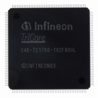
SAK-TC1766-192F80HL BD Infineon Technologies, SAK-TC1766-192F80HL BD Datasheet - Page 54

SAK-TC1766-192F80HL BD
Manufacturer Part Number
SAK-TC1766-192F80HL BD
Description
IC MCU 32BIT FLASH PG-LQFP-176
Manufacturer
Infineon Technologies
Series
TC17xxr
Datasheet
1.SAK-TC1766-192F80HL_BD.pdf
(117 pages)
Specifications of SAK-TC1766-192F80HL BD
Core Processor
TriCore
Core Size
32-Bit
Speed
80MHz
Connectivity
ASC, CAN, MLI, MSC, SSC
Peripherals
DMA, POR, WDT
Number Of I /o
81
Program Memory Size
1.5MB (1.5M x 8)
Program Memory Type
FLASH
Ram Size
108K x 8
Voltage - Supply (vcc/vdd)
1.42 V ~ 1.58 V
Data Converters
A/D 2x10b; A/D 32x8b,10b,12b
Oscillator Type
External
Operating Temperature
-40°C ~ 125°C
Package / Case
176-LFQFP
Packages
PG-LQFP-176
Max Clock Frequency
80.0 MHz
Sram (incl. Cache)
108.0 KByte
Can Nodes
2
A / D Input Lines (incl. Fadc)
36
Program Memory
1.5 MB
For Use With
B158-H8539-G2-X-7600IN - KIT STARTER TC176X SERIES
Lead Free Status / RoHS Status
Lead free / RoHS Compliant
Eeprom Size
-
Other names
KT1766192F80HLBDXT
SAK-TC1766-192F80HLBDINTR
SAK-TC1766-192F80HLBDINTR
Preliminary
3.14
Section 3.14
interfaces and the features which are provided by the module.
Figure 3-11 Block Diagram of the ADC Module
The ADC module has 16 analog input channels. An analog multiplexer selects the input
line for the analog input channels from among 32 analog inputs. Additionally, an external
analog multiplexer can be used for analog input extension. External Clock control,
address decoding, and service request (interrupt) control are managed outside the ADC
module kernel. External trigger conditions are controlled by an External Request Unit.
This unit generates the control signals for auto-scan control (ASGT), software trigger
control (SW0TR, SW0GT), the event trigger control (ETR, EGT), queue control (QTR,
QGT), and timer trigger control (TTR, TGT).
An automatic self-calibration adjusts the ADC module to changing temperatures or
process variations.
functional blocks and interfaces.
Data Sheet
Decoder
To DMA
Address
Interrupt
Control
Control
Clock
Analog-to-Digital Converter (ADC0)
SR[3:0]
SR[7:4]
f
f
ADC
CLC
shows the global view of the ADC module with its functional blocks and
V
AGND0
Figure 3-11
V
DD
V
Module
Kernel
ADC0
SS
V
SSM
V
DDM
shows the global view of the ADC module with its
V
AREF0
Group 1
SW0TR, SW0GT
QTR, QGT
TTR, TGT
Group 0
ETR, EGT
ASGT
GPRS
EMUX0
EMUX1
50
0
1
AIN0
AIN15
AIN16
AIN30
AIN31
Measurement
Temperature
External
Request
Control
(SCU)
Port 1
Unit
Die
Functional Description
8
2
6
SCU_CON.DTSON
A1
A1
A1
D
D
D
D
D
P1.14 /
AD0EMUX2 (GRPS)
P1.13 /AD0EMUX1
P1.12 /AD0EMUX0
From Ports
From MSC0
From GPTA
AN0
AN15
AN16
AN30
AN31
V1.0, 2008-04
TC1766
MCA06427


