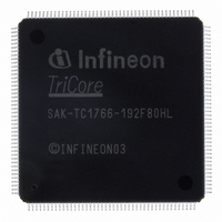
SAK-TC1766-192F80HL BD Infineon Technologies, SAK-TC1766-192F80HL BD Datasheet - Page 67

SAK-TC1766-192F80HL BD
Manufacturer Part Number
SAK-TC1766-192F80HL BD
Description
IC MCU 32BIT FLASH PG-LQFP-176
Manufacturer
Infineon Technologies
Series
TC17xxr
Datasheet
1.SAK-TC1766-192F80HL_BD.pdf
(117 pages)
Specifications of SAK-TC1766-192F80HL BD
Core Processor
TriCore
Core Size
32-Bit
Speed
80MHz
Connectivity
ASC, CAN, MLI, MSC, SSC
Peripherals
DMA, POR, WDT
Number Of I /o
81
Program Memory Size
1.5MB (1.5M x 8)
Program Memory Type
FLASH
Ram Size
108K x 8
Voltage - Supply (vcc/vdd)
1.42 V ~ 1.58 V
Data Converters
A/D 2x10b; A/D 32x8b,10b,12b
Oscillator Type
External
Operating Temperature
-40°C ~ 125°C
Package / Case
176-LFQFP
Packages
PG-LQFP-176
Max Clock Frequency
80.0 MHz
Sram (incl. Cache)
108.0 KByte
Can Nodes
2
A / D Input Lines (incl. Fadc)
36
Program Memory
1.5 MB
For Use With
B158-H8539-G2-X-7600IN - KIT STARTER TC176X SERIES
Lead Free Status / RoHS Status
Lead free / RoHS Compliant
Eeprom Size
-
Other names
KT1766192F80HLBDXT
SAK-TC1766-192F80HLBDINTR
SAK-TC1766-192F80HLBDINTR
Preliminary
3.22
The TC1766 clock system performs the following functions:
•
•
•
•
•
•
The clock system must be operational before the TC1766 can function, so it contains
special logic to handle power-up and reset operations. Its services are fundamental to
the operation of the entire system, so it contains special fail-safe logic.
Features
•
•
•
•
The TC1766 Clock Generation Unit (CGU) as shown in
flexible clock generation. It basically consists of an main oscillator circuit and a Phase-
Locked Loop (PLL). The PLL can converts a low-frequency external clock signal from the
oscillator circuit to a high-speed internal clock for maximum performance.
The system clock
hardware/software selectable ways:
•
•
•
•
Data Sheet
Acquires and buffers incoming clock signals to create a master clock frequency
Distributes in-phase synchronized clock signals throughout the TC1766’s entire clock
tree
Divides a system master clock frequency into lower frequencies required by the
different modules for operation.
Dynamically reduces power consumption during operation of functional units
Statically reduces power consumption through programmable power-saving modes
Reduces electromagnetic interference (EMI) by switching off unused modules
PLL operation for multiplying clock source by different factors
Direct drive capability for direct clocking
Comfortable state machine for secure switching between basic PLL, direct or
prescaler operation
Sleep and Power-Down Mode support
Direct Drive Mode (PLL Bypass):
In Direct Drive Mode, the TC1766 clock system is directly driven by an external clock
signal. input, i.e.
a reasonably small fundamental mode crystal.
VCO Bypass Mode (Prescaler Mode):
In VCO Bypass Mode,
P-Divider and K-Divider. The system clock
PLL Mode:
In PLL Mode, the PLL is running. The VCO clock
the P factor, multiplied by the PLL (N-Divider). The clock signals
derived from
PLL Base Mode:
In PLL Base Mode, the PLL is running at its VCO base frequency and
Clock Generation and PLL
f
VCO
f
SYS
f
CPU
by the K-Divider. The system clock
is generated from an oscillator clock
=
f
f
CPU
OSC
and
and
f
f
SYS
SYS
=
are derived from
f
OSC
63
. This allows operation of the TC1766 with
f
SYS
is equal to
f
VCO
is derived from
f
f
SYS
OSC
f
OSC
Figure 3-15
is equal to
by the two divider stages,
f
CPU
Functional Description
in either one of the four
.
f
CPU
f
f
OSC
CPU
allows a very
f
V1.0, 2008-04
and
CPU
, divided by
.
TC1766
and
f
SYS
f
are
SYS


