OP470GPZ Analog Devices Inc, OP470GPZ Datasheet - Page 5
OP470GPZ
Manufacturer Part Number
OP470GPZ
Description
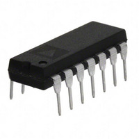
IC OPAMP GP 6MHZ QUAD LN 14DIP
Manufacturer
Analog Devices Inc
Specifications of OP470GPZ
Slew Rate
2 V/µs
Amplifier Type
General Purpose
Number Of Circuits
4
Gain Bandwidth Product
6MHz
Current - Input Bias
25nA
Voltage - Input Offset
400µV
Current - Supply
9mA
Voltage - Supply, Single/dual (±)
9 V ~ 36 V, ±4.5 V ~ 18 V
Operating Temperature
-40°C ~ 85°C
Mounting Type
Through Hole
Package / Case
14-DIP (0.300", 7.62mm)
Op Amp Type
General Purpose
No. Of Amplifiers
4
Bandwidth
6MHz
Supply Voltage Range
± 4.5V To ± 18V
Amplifier Case Style
DIP
No. Of Pins
14
Channel Separation
125
Common Mode Rejection Ratio
100
Current, Input Bias
25 nA
Current, Input Offset
12 nA
Current, Supply
9 mA
Impedance, Thermal
33 °C/W
Number Of Amplifiers
Quad
Package Type
PDIP-14
Resistance, Input
0.4 Megohms (Differential), 11 Gigaohms (Common-Mode)
Temperature, Operating, Range
-40 to +85 °C
Voltage, Gain
1700 V/mV
Voltage, Input
±11, ±12 V
Voltage, Noise
3.8 nV/sqrt Hz
Voltage, Offset
0.4 mV
Voltage, Output, High
+13 V
Voltage, Output, Low
-13 V
Voltage, Supply
±15 V
Lead Free Status / RoHS Status
Lead free / RoHS Compliant
Output Type
-
Current - Output / Channel
-
-3db Bandwidth
-
Lead Free Status / Rohs Status
RoHS Compliant part
Electrostatic Device
Available stocks
Company
Part Number
Manufacturer
Quantity
Price
Company:

Part Number:
OP470GPZ
Manufacturer:
AD
Quantity:
1 200
Part Number:
OP470GPZ
Manufacturer:
ADI/亚德诺
Quantity:
20 000


T
V
( V)
400
400
400
800
1000
1000
*Not for new design; obsolete April 2002.
For military processed devices, please refer to the standard
Microcircuit Drawing (SMD) available at
www.dscc.dla.mil/programs/milspec/default.asp
SMD Part Number
59628856501CA
596288565012A
596288565013A
* Not for new designs; obsolete April 2002.
ABSOLUTE MAXIMUM RATINGS
Supply Voltage . . . . . . . . . . . . . . . . . . . . . . . . . . . . . . . . ± 18 V
Differential Input Voltage
Differential Input Current
Input Voltage . . . . . . . . . . . . . . . . . . . . . . . . . . Supply Voltage
Output Short-Circuit Duration . . . . . . . . . . . . . . . Continuous
Storage Temperature Range
Lead Temperature Range (Soldering 60 sec) . . . . . . . . . 300∞C
Junction Temperature (T
Operating Temperature Range
CAUTION
ESD (electrostatic discharge) sensitive device. Electrostatic charges as high as 4000 V readily
accumulate on the human body and test equipment and can discharge without detection. Although
the OP470 features proprietary ESD protection circuitry, permanent damage may occur on devices
subjected to high energy electrostatic discharges. Therefore, proper ESD precautions are
recommended to avoid performance degradation or loss of functionality.
REV. B
A
OS
P, Y Package . . . . . . . . . . . . . . . . . . . . . . –65∞C to +150∞C
OP470A . . . . . . . . . . . . . . . . . . . . . . . . . –55∞C to +125∞C
OP470E, OP470F . . . . . . . . . . . . . . . . . . . –25∞C to +85∞C
OP470G . . . . . . . . . . . . . . . . . . . . . . . . . . –40∞C to +85∞C
= 25∞C
max
*
Cerdip
14-Pin
OP470AY*
OP470EY
OP470FY*
ORDERING GUIDE
Package Options
j
2
) . . . . . . . . . . . . . –65∞C to +150∞C
2
. . . . . . . . . . . . . . . . . . . . . . ± 1.0 V
. . . . . . . . . . . . . . . . . . . . ± 25 mA
Plastic
OP470GP
OP470GS
1
ADI Equivalent
OP470AYMDA
OP470ARCMDA
OP470ATCMDA
Operating
Range
MIL
IND
IND
XIND
Temperature
MIL
XIND
–5–
Package Type
14-Lead Hermetic DIP(Y) 94
14-Lead Plastic DIP(P)
16-Lead SOIC (S)
NOTES
1
2
3
OUT B
OUT C
Absolute Maximum Ratings apply to both DICE and packaged parts, unless
The OP470’s inputs are protected by back-to-back diodes. Current limiting
–IN B
otherwise noted.
resistors are not used in order to achieve low noise performance. If differential
voltage exceeds ± 1.0 V, the input current should be limited to ± 25 mA.
in socket for TO, CerDIP, PDIP, packages;
printed circuit board for SOIC packages.
JA
is specified for worst case mounting conditions, i.e.,
–IN C +IN C
+IN B
DIE SIZE 0.163
Figure 1. Dice Characteristics
(4.14
2.69 mm, 11.14 SQ. mm)
0.106 INCH, 17,278 SQ. mm
76
88
JA
V+
V–
3
WARNING!
JA
is specified for device soldered to
ESD SENSITIVE DEVICE
JA
10
33
23
JC
is specified for device
+IN A
+IN D
OP470
∞C/W
∞C/W
∞C/W
Unit
–IN A
OUT A
OUT D
–IN D
Related parts for OP470GPZ
Image
Part Number
Description
Manufacturer
Datasheet
Request
R

Part Number:
Description:
±1.7g Dual-Axis IMEMS Accelerometer Evaluation Board
Manufacturer:
Analog Devices Inc
Datasheet:

Part Number:
Description:
Inertial Sensor Evaluation System
Manufacturer:
Analog Devices Inc
Datasheet:
Part Number:
Description:
Manufacturer:
Analog Devices Inc
Datasheet:
Part Number:
Description:
Manufacturer:
Analog Devices Inc
Datasheet:
Part Number:
Description:
Manufacturer:
Analog Devices Inc
Datasheet:
Part Number:
Description:
Manufacturer:
Analog Devices Inc
Datasheet:
Part Number:
Description:
Manufacturer:
Analog Devices Inc
Datasheet:
Part Number:
Description:
Manufacturer:
Analog Devices Inc
Datasheet:
Part Number:
Description:
Manufacturer:
Analog Devices Inc
Datasheet:
Part Number:
Description:
Manufacturer:
Analog Devices Inc
Datasheet:
Part Number:
Description:
Manufacturer:
Analog Devices Inc
Datasheet:
Part Number:
Description:
Manufacturer:
Analog Devices Inc
Datasheet:
Part Number:
Description:
Manufacturer:
Analog Devices Inc
Datasheet: