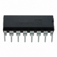
SMP04EPZ Analog Devices Inc, SMP04EPZ Datasheet - Page 13

SMP04EPZ
Manufacturer Part Number
SMP04EPZ
Description
IC AMP SAMPLE HOLD CMOS 16DIP
Manufacturer
Analog Devices Inc
Datasheet
1.SMP04ESZ.pdf
(15 pages)
Specifications of SMP04EPZ
Amplifier Type
Sample and Hold
Number Of Circuits
4
Slew Rate
4 V/µs
Current - Input Bias
500nA
Voltage - Input Offset
2500µV
Current - Supply
4mA
Current - Output / Channel
1.2mA
Voltage - Supply, Single/dual (±)
5 V ~ 12 V, ±2.5 V ~ 6 V
Operating Temperature
-40°C ~ 85°C
Mounting Type
Through Hole
Package / Case
16-DIP (0.300", 7.62mm)
No. Of Amplifiers
4
Bandwidth
85kHz
Acquisition Time
9µs
Input Offset Voltage
2.5mV
Settling Time
3.5µs
Supply Voltage Range
10.8V To 13.2V, ± 5V To ± 6V
Amplifier Case Style
DIP
Lead Free Status / RoHS Status
Lead free / RoHS Compliant
Output Type
-
-3db Bandwidth
-
Gain Bandwidth Product
-
Lead Free Status / RoHS Status
Lead free / RoHS Compliant, Lead free / RoHS Compliant
Available stocks
Company
Part Number
Manufacturer
Quantity
Price
Company:
Part Number:
SMP04EPZ
Manufacturer:
FUJ
Quantity:
6 227
D/A CONVERTER DEGLITCHER
Most D/A converters output an appreciable amount of glitch
energy during a transition from one code to another. The glitch
amplitude can range from several millivolts to hundreds of milli-
volts. This may become unacceptable in many applications. By
selectively delaying the DAC’s output transition, the SMP04
can be used to smooth the output waveform. Figure 25 shows
the schematic diagram of such a deglitcher circuit. Two simple
logic gates (an OR and a NAND gate) provide the proper timing
sequence for the DAC WR strobe and the S/H control signal to
the SMP04. In this example a linear ramp signal is generated by
feeding the most significant eight bits of the 10-bit binary
counter to the DAC. The two least significant bits are used to
produce the delayed WR strobe and the S/H control signals.
Referring to Figure 26a, new data to the DAC input is set up at
the S/H’s falling edge, but the DAC output does not change
until a WR strobe goes active. During this period, the SMP04 is
in a sample mode whose output tracks the DAC output. When
S/H goes HIGH, the current DAC output voltage is held by the
SMP04. After 1.2 s settling, the WR strobe goes LOW to allow
the DAC output to change. Any glitch that occurs at the DAC
output is effectively blocked by the SMP04. As soon as the WR
strobe goes HIGH, the digital data is latched; at the same time
the S/H goes LOW, allowing the SMP04 to track to the new
DAC output voltage.
Figure 26b shows the deglitching operation. The top trace
shows the DAC output during a transition, while the bottom
trace shows the deglitched output of the SMP04.
REV. D
GENERATOR
COUNTER
CLOCK
10-BIT
DB
+5V
2
–DB
DB
DB
ANALOG
RETURN
RETURN
DIGITAL
0
1
9
DB
DB
9
2
A
A
1
0
MSB
LSB
V
SS
+15V
V
Figure 25. DAC Deglitcher
DD
DEGLITCH LOGIC
1/4 DAC8426
AGND
1/4 AD7432
0.1 F
DGND
–13–
V
OUT
WR
REF
1/4 AD7400
Figure 26. (a) Shows the Logic Timing of the Deglitcher.
The Top Two Traces Are the Two Least Significant Bits,
DB
the WR and S /H Signals Which Are Shown in the Bottom
Two Traces. (b) Shows the Typical Glitch Amplitude of a
DAC (Top Trace) and the Deglitched Output of the AMP04
(Bottom Trace).
0
DAC C
and DB
OUT
1
0.1 F–1 F CERAMIC
V
S/H
, Respectively. These Are Used to Generate
IN
DGND
1/4 SMP04
5V
50m
V
SS
a.
DLY
b.
+15V
V
DD
1 s
627.4
1 F
AGND
1 s
V
OUT
s
SMP04
DB
DB
WR
S/H
0
1


