OP470EY Analog Devices Inc, OP470EY Datasheet - Page 4
OP470EY
Manufacturer Part Number
OP470EY
Description
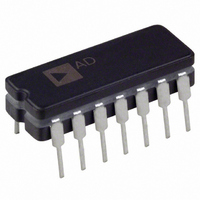
IC OPAMP GP 6MHZ QUAD LN 14CDIP
Manufacturer
Analog Devices Inc
Datasheet
1.OP470GPZ.pdf
(16 pages)
Specifications of OP470EY
Slew Rate
2 V/µs
Rohs Status
RoHS non-compliant
Amplifier Type
General Purpose
Number Of Circuits
4
Gain Bandwidth Product
6MHz
Current - Input Bias
6nA
Voltage - Input Offset
100µV
Current - Supply
9mA
Voltage - Supply, Single/dual (±)
9 V ~ 36 V, ±4.5 V ~ 18 V
Operating Temperature
-25°C ~ 85°C
Mounting Type
Through Hole
Package / Case
14-CDIP (0.300", 7.62mm)
Op Amp Type
General Purpose
No. Of Amplifiers
4
Bandwidth
6MHz
Supply Voltage Range
± 4.5V To ± 18V
Amplifier Case Style
DIP
No. Of Pins
14
Output Type
-
Current - Output / Channel
-
-3db Bandwidth
-
Lead Free Status / RoHS Status
Contains lead / RoHS non-compliant
Available stocks
Company
Part Number
Manufacturer
Quantity
Price

Part Number:
OP470EY
Manufacturer:
PMI
Quantity:
20 000


OP470–SPECIFICATIONS
WAFER TEST LIMITS
Parameter
INPUT OFFSET VOLTAGE
INPUT OFFSET CURRENT
INPUT BIAS CURRENT
LARGE-SIGNAL
INPUT VOLTAGE RANGE
OUTPUT VOLTAGE SWING
COMMON-MODE
REJECTION
POWER SUPPLY
REJECTION RATIO
SUPPLY CURRENT
NOTE
*
Electrical tests are performed at wafer probe to the limits shown. Due to variations in assembly methods and normal yield loss, yield after packaging is not guaran-
teed for standard product dice. Consult factory to negotiate specifications based on dice lot qualification through sample lot assembly and testing.
Guaranteed by CMR test
Voltage Gain
(All Amplifiers)
*
(at V
S
Symbol
V
I
I
A
IVR
V
CMR
PSRR
I
=
OS
B
SY
OS
VO
O
15 V, 25 C, unless otherwise noted.)
Conditions
V
V
V
R
R
R
V
V
No Load
CM
CM
O
L
L
L
CM
S
≥ 2 kW
= ± 4.5 V to ± 18 V
= 10 kW
= 2 kW
= ± 10 V
= ± 11 V
= 0 V
= 0 V
–4–
OP470GBC
Limit
0.8
20
50
800
400
± 11
± 12
100
5.6
11
Unit
mV Max
nA Max
nA Min
V/mV Min
V Min
V Min
dB
mV/V Max
mA Max
REV. B
Related parts for OP470EY
Image
Part Number
Description
Manufacturer
Datasheet
Request
R

Part Number:
Description:
IC OPAMP INSTR PREC SGL 8SOIC
Manufacturer:
Linear Technology
Datasheet:

Part Number:
Description:
Op Amps Low-noise op amp Noise Wide-Band Ampl
Manufacturer:
Maxim Integrated Products
Datasheet:

Part Number:
Description:
Op Amps LW-POW SNGL/DUAL R-R I/O OP AMPS
Manufacturer:
Maxim Integrated Products
Datasheet:
Part Number:
Description:
Op Amps LW-POW SNGL/DUAL R-R I/O OP AMPS
Manufacturer:
Maxim Integrated Products
Datasheet:

Part Number:
Description:
Op Amps Dual Op amp JFET
Manufacturer:
Fairchild Semiconductor
Datasheet:

Part Number:
Description:
Op Amps 1.8V 15MHz Low-Offse set Op Amp with RRIO
Manufacturer:
Maxim Integrated Products
Datasheet:

Part Number:
Description:
Op Amps Ultra low-power op a mp in 6-bump WLP pac
Manufacturer:
Maxim Integrated Products
Datasheet:
Part Number:
Description:
Op Amps 1.8V 15MHz Low-Offse set Op Amp with RRIO
Manufacturer:
Maxim Integrated Products
Datasheet:

Part Number:
Description:
Op Amps Dual High-Voltage Op Amp
Manufacturer:
Maxim Integrated Products
Datasheet:


