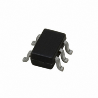
LMV821M7/NOPB National Semiconductor, LMV821M7/NOPB Datasheet - Page 12

LMV821M7/NOPB
Manufacturer Part Number
LMV821M7/NOPB
Description
IC OP AMP R-R LOW V LP SC-70-5
Manufacturer
National Semiconductor
Datasheet
1.LMV821M5NOPB.pdf
(24 pages)
Specifications of LMV821M7/NOPB
Amplifier Type
General Purpose
Number Of Circuits
1
Output Type
Rail-to-Rail
Slew Rate
2 V/µs
Gain Bandwidth Product
5.6MHz
Current - Input Bias
100nA
Voltage - Input Offset
3500µV
Current - Supply
300µA
Current - Output / Channel
45mA
Voltage - Supply, Single/dual (±)
2.5 V ~ 5.5 V, ±1.25 V ~ 2.75 V
Operating Temperature
-40°C ~ 85°C
Mounting Type
Surface Mount
Package / Case
SC-70-5, SC-88A, SOT-323-5, SOT-353, 5-TSSOP
Lead Free Status / RoHS Status
Lead free / RoHS Compliant
-3db Bandwidth
-
Other names
LMV821M7
LMV821M7TR
LMV821M7TR
Available stocks
Company
Part Number
Manufacturer
Quantity
Price
Company:
Part Number:
LMV821M7/NOPB
Manufacturer:
NS
Quantity:
316 000
Company:
Part Number:
LMV821M7/NOPB
Manufacturer:
NSC
Quantity:
2 848
www.national.com
Application Note
UNITY GAIN PULSE RESPONSE CONSIDERATION
A pull-up resistor is well suited for increasing unity-gain,
pulse response stability. For example, a 600 Ω pull-up resis-
tor reduces the overshoot voltage by about 50%, when
driving a 220 pF load. Figure 3 shows how to implement the
pull-up resistor for more pulse response stability.
Higher capacitances can be driven by decreasing the value
of the pull-up resistor, but its value shouldn’t be reduced
beyond the sinking capability of the part. An alternate ap-
proach is to use an isolation resistor as illustrated in Figure 4
.
Figure 5 shows the resulting pulse response from a LMV824,
while driving a 10,000 pF load through a 20Ω isolation
resistor.
FIGURE 4. Using an Isolation Resistor to Drive Heavy
FIGURE 3. Using a Pull-up Resistor at the Output for
FIGURE 2. Unity-Gain Frequency vs Common Mode
Stabilizing Capacitive Loads
Voltage for Various Loads
Capacitive Loads
(Continued)
10012841
10012861
10012843
12
INPUT BIAS CURRENT CONSIDERATION
Input bias current (I
offset voltage. This offset is primarily due to I
through the negative feedback resistor, R
is 90 nA (max
mV will be developed (V
resistor (R
But the input offset current (I
offset voltage in the same manner - typically 0.05 mV at
room temp.
APPLICATION CIRCUITS
This section covers the following application circuits:
1. Telephone-Line Transceiver
2. “Simple” Mixer (Amplitude Modulator)
FIGURE 6. Canceling the Voltage Offset Effect of Input
FIGURE 5. Pulse Response per Figure 4
C
), as shown in Figure 6, cancels out this affect.
@
room) and R
B
) can develop a somewhat significant
Bias Current
OS
=I
F
B
OS
is 100 kΩ, then an offset of 9
x R
) will still contribute to an
F
).Using a compensation
F
. For example, if I
10012854
10012859
B
flowing
B


