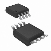
LMP7702MM/NOPB National Semiconductor, LMP7702MM/NOPB Datasheet - Page 15

LMP7702MM/NOPB
Manufacturer Part Number
LMP7702MM/NOPB
Description
IC AMP PREC R-R I/O DUAL 8-MSOP
Manufacturer
National Semiconductor
Series
LMP®r
Type
General Purpose Amplifierr
Datasheet
1.LMP7701MFNOPB.pdf
(24 pages)
Specifications of LMP7702MM/NOPB
Amplifier Type
General Purpose
Number Of Circuits
2
Output Type
Rail-to-Rail
Slew Rate
1.1 V/µs
Gain Bandwidth Product
2.5MHz
Current - Input Bias
0.2pA
Voltage - Input Offset
37µV
Current - Supply
1.7mA
Current - Output / Channel
86mA
Voltage - Supply, Single/dual (±)
2.7 V ~ 12 V, ±1.35 V ~ 6 V
Operating Temperature
-40°C ~ 125°C
Mounting Type
Surface Mount
Package / Case
8-MSOP, Micro8™, 8-uMAX, 8-uSOP,
Rail/rail I/o Type
Rail to Rail Input/Output
Number Of Elements
2
Unity Gain Bandwidth Product
2.5MHz
Common Mode Rejection Ratio
86dB
Input Offset Voltage
220uV
Input Bias Current
1pA
Single Supply Voltage (typ)
3/5/9V
Dual Supply Voltage (typ)
Not RequiredV
Voltage Gain In Db
130dB
Power Supply Rejection Ratio
86dB
Power Supply Requirement
Single
Shut Down Feature
No
Single Supply Voltage (min)
2.7V
Single Supply Voltage (max)
12V
Dual Supply Voltage (min)
Not RequiredV
Dual Supply Voltage (max)
Not RequiredV
Technology
CMOS
Operating Temp Range
-40C to 125C
Operating Temperature Classification
Automotive
Mounting
Surface Mount
Pin Count
8
Package Type
MSOP
Lead Free Status / RoHS Status
Lead free / RoHS Compliant
-3db Bandwidth
-
Lead Free Status / Rohs Status
Compliant
Other names
LMP7702MM
LMP7702MMTR
LMP7702MMTR
Available stocks
Company
Part Number
Manufacturer
Quantity
Price
Part Number:
LMP7702MM/NOPB
Manufacturer:
NS/国半
Quantity:
20 000
Application Information
LMP7701/LMP7702/LMP7704
The LMP7701/LMP7702/LMP7704 are single, dual, and quad
low offset voltage, rail-to-rail input and output precision am-
plifiers each with a CMOS input stage and wide supply voltage
range of 2.7V to 12V. The LMP7701/LMP7702/LMP7704
have a very low input bias current of only ±200 fA at room
temperature.
The wide supply voltage range of 2.7V to 12V over the ex-
tensive temperature range of −40°C to 125°C makes the
LMP7701/LMP7702/LMP7704 excellent choices for low volt-
age precision applications with extensive temperature re-
quirements.
The LMP7701/LMP7702/LMP7704 have only ±37 μV of typ-
ical input referred offset voltage and this offset is guaranteed
to be less than ±500 μV for the single and ±520 μV for the
dual and quad, over temperature. This minimal offset voltage
allows more accurate signal detection and amplification in
precision applications.
The low input bias current of only ±200 fA along with the low
input referred voltage noise of 9 nV/
LMP7702/LMP7704 superiority for use in sensor applications.
Lower levels of noise from the LMP7701/LMP7702/LMP7704
mean of better signal fidelity and a higher signal-to-noise ra-
tio.
National Semiconductor is heavily committed to precision
amplifiers and the market segment they serve. Technical sup-
port and extensive characterization data is available for sen-
sitive applications or applications with a constrained error
budget.
The LMP7701 is offered in the space saving 5-Pin SOT23 and
8-Pin SOIC package. The LMP7702 comes in the 8-Pin SOIC
and 8-Pin MSOP package. The LMP7704 is offered in the 14-
Pin SOIC and 14-Pin TSSOP package. These small pack-
ages are ideal solutions for area constrained PC boards and
portable electronics.
CAPACITIVE LOAD
The LMP7701/LMP7702/LMP7704 can each be connected
as a non-inverting unity gain follower. This configuration is the
most sensitive to capacitive loading.
The combination of a capacitive load placed on the output of
an amplifier along with the amplifier's output impedance cre-
ates a phase lag which in turn reduces the phase margin of
the amplifier. If the phase margin is significantly reduced, the
response will be either underdamped or it will oscillate.
In order to drive heavier capacitive loads, an isolation resistor,
R
sistor, the capacitive load is isolated from the amplifier's
output, and hence, the pole caused by C
feedback loop. The larger the value of R
the output voltage will be. If values of R
large, the feedback loop will be stable, independent of the
value of C
output swing and reduced output current drive.
ISO
, in Figure 1 should be used. By using this isolation re-
L
. However, larger values of R
ISO
gives the LMP7701/
ISO
L
ISO
is no longer in the
, the more stable
result in reduced
are sufficiently
15
INPUT CAPACITANCE
CMOS input stages inherently have low input bias current and
higher input referred voltage noise. The LMP7701/LMP7702/
LMP7704 enhance this performance by having the low input
bias current of only ±200 fA, as well as, a very low input re-
ferred voltage noise of 9 nV/
larger input stage has been used. This larger input stage in-
creases the input capacitance of the LMP7701/LMP7702/
LMP7704. The typical value of this input capacitance, C
the LMP7701/LMP7702/LMP7704 is 25 pF. The input capac-
itance will interact with other impedances such as gain and
feedback resistors, which are seen on the inputs of the am-
plifier, to form a pole. This pole will have little or no effect on
the output of the amplifier at low frequencies and DC condi-
tions, but will play a bigger role as the frequency increases.
At higher frequencies, the presence of this pole will decrease
phase margin and will also cause gain peaking. In order to
compensate for the input capacitance, care must be taken in
choosing the feedback resistors. In addition to being selective
in picking values for the feedback resistor, a capacitor can be
added to the feedback path to increase stability.
The DC gain of the circuit shown in Figure 2 is simply –R
R
For the time being, ignore C
Figure 2 can be calculated as follows:
1
.
FIGURE 2. Compensating for Input Capacitance
FIGURE 1. Isolating Capacitive Load
F
. The AC gain of the circuit in
. In order to achieve this a
20127321
20127344
www.national.com
IN
, for
2
/


