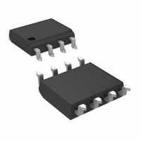
LM6132BIM/NOPB National Semiconductor, LM6132BIM/NOPB Datasheet - Page 12

LM6132BIM/NOPB
Manufacturer Part Number
LM6132BIM/NOPB
Description
IC OP AMP DUAL H SPEED LP 8-SOIC
Manufacturer
National Semiconductor
Specifications of LM6132BIM/NOPB
Amplifier Type
General Purpose
Number Of Circuits
2
Output Type
Rail-to-Rail
Slew Rate
14 V/µs
Gain Bandwidth Product
11MHz
Current - Input Bias
125nA
Voltage - Input Offset
1700µV
Current - Supply
390µA
Current - Output / Channel
4mA
Voltage - Supply, Single/dual (±)
1.8 V ~ 24 V, ±0.9 V ~ 12 V
Operating Temperature
-40°C ~ 85°C
Mounting Type
Surface Mount
Package / Case
8-SOIC (3.9mm Width)
Bandwidth
10 MHz
Common Mode Rejection Ratio
80
Current, Input Bias
110 nA
Current, Input Offset
3.4 nA
Current, Output
4 mA
Current, Supply
360 μA
Harmonic Distortion
0.0015 %
Impedance, Thermal
193 °C/W
Number Of Amplifiers
Dual
Package Type
SO-8
Resistance, Input
104 Megohms
Temperature, Operating, Range
-40 to +85 °C
Voltage, Gain
100 V/mV
Voltage, Input
1.8 to 24 V
Voltage, Noise
27 nV/sqrt Hz
Voltage, Offset
0.25 mV
Voltage, Output, High
4.992 V
Voltage, Output, Low
0.007 V
Voltage, Supply
5 V
Number Of Channels
2
Voltage Gain Db
100 dB
Common Mode Rejection Ratio (min)
60 dB
Input Offset Voltage
6 mV at 5 V
Operating Supply Voltage
3 V, 5 V, 9 V, 12 V, 15 V, 18 V
Supply Current
0.8 mA at 5 V
Maximum Operating Temperature
+ 85 C
Minimum Operating Temperature
- 40 C
Lead Free Status / RoHS Status
Lead free / RoHS Compliant
-3db Bandwidth
-
Lead Free Status / Rohs Status
RoHS Compliant part
Electrostatic Device
Other names
*LM6132BIM
*LM6132BIM/NOPB
LM6132BIM
*LM6132BIM/NOPB
LM6132BIM
www.national.com
LM6132/34 Application Information
Figure 6 shows a method for compensating for load capaci-
tance (C
(Continued)
O
) effects by adding both an isolation resistor R
FIGURE 3.
FIGURE 4.
FIGURE 5.
01234943
01234945
01234942
O
at
12
the output and a feedback capacitor C
output and the inverting input pin. Feedback capacitor C
compensates for the pole introduced by R
mizing ringing in the output waveform while the feedback
resistor R
R
of R
Typical Applications
3 OP AMP INSTRUMENTATION AMP WITH
RAIL-TO-RAIL INPUT AND OUTPUT
Using the LM6134, a 3 op amp instrumentation amplifier with
rail-to-rail inputs and rail to rail output can be made. These
features make these instrumentation amplifiers ideal for
single supply systems.
Some manufacturers use a precision voltage divider array of
5 resistors to divide the common-mode voltage to get an
input range of rail-to-rail or greater. The problem with this
method is that it also divides the signal, so to even get unity
gain, the amplifier must be run at high closed loop gains.
This raises the noise and drift by the internal gain factor and
lowers the input impedance. Any mismatch in these preci-
sion resistors reduces the CMR as well. Using the LM6134,
all of these problems are eliminated.
In this example, amplifiers A and B act as buffers to the
differential stage (Figure 7). These buffers assure that the
input impedance is over 100 MΩ and they eliminate the
requirement for precision matched resistors in the input
stage. They also assure that the difference amp is driven
from a voltage source. This is necessary to maintain the
CMR set by the matching of R1–R2 with R3–R4.
O
. Depending on the size of the load capacitance, the value
O
is typically chosen to be between 100Ω to 1 kΩ.
F
compensates for dc inaccuracies introduced by
FIGURE 6.
FIGURE 7.
F
directly between the
O
and C
01234937
O
01234944
, mini-
F


