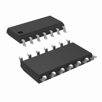
LMH6644MA/NOPB National Semiconductor, LMH6644MA/NOPB Datasheet - Page 5

LMH6644MA/NOPB
Manufacturer Part Number
LMH6644MA/NOPB
Description
IC AMP R-R I/O 3V 130MHZ 14-SOIC
Manufacturer
National Semiconductor
Series
PowerWise®r
Type
Voltage Feedback Amplifierr
Datasheet
1.LMH6642MFNOPB.pdf
(22 pages)
Specifications of LMH6644MA/NOPB
Amplifier Type
Voltage Feedback
Number Of Circuits
4
Output Type
Rail-to-Rail
Slew Rate
135 V/µs
-3db Bandwidth
130MHz
Current - Input Bias
20nA
Voltage - Input Offset
1000µV
Current - Supply
2.7mA
Current - Output / Channel
75mA
Voltage - Supply, Single/dual (±)
2.7 V ~ 12.8 V, ±1.35 V ~ 6.4 V
Operating Temperature
-40°C ~ 85°C
Mounting Type
Surface Mount
Package / Case
14-SOIC (3.9mm Width), 14-SOL
Rail/rail I/o Type
Rail to Rail Output
Number Of Elements
4
Common Mode Rejection Ratio
72dB
Input Offset Voltage
5mV
Input Bias Current
2.6uA
Single Supply Voltage (typ)
3/5/9/12V
Dual Supply Voltage (typ)
±3/±5V
Voltage Gain In Db
98dB
Power Supply Rejection Ratio
79dB
Power Supply Requirement
Single/Dual
Shut Down Feature
No
Single Supply Voltage (min)
2.7V
Single Supply Voltage (max)
12.8V
Dual Supply Voltage (min)
±1.35V
Dual Supply Voltage (max)
±6.4V
Technology
BiCOM
Operating Temp Range
-40C to 85C
Operating Temperature Classification
Industrial
Mounting
Surface Mount
Pin Count
14
Package Type
SOIC N
Number Of Channels
4
Voltage Gain Db
98 dB
Common Mode Rejection Ratio (min)
72 dB
Input Voltage Range (max)
12.8 V
Input Voltage Range (min)
2.7 V
Operating Supply Voltage
3 V, 5 V, 9 V, 12 V
Supply Current
17 mA at 5 V
Maximum Operating Temperature
+ 85 C
Mounting Style
SMD/SMT
Maximum Dual Supply Voltage
+/- 6.4 V
Minimum Operating Temperature
- 40 C
Lead Free Status / RoHS Status
Lead free / RoHS Compliant
Gain Bandwidth Product
-
Lead Free Status / Rohs Status
Compliant
Other names
*LMH6644MA
*LMH6644MA/NOPB
LMH6644MA
*LMH6644MA/NOPB
LMH6644MA
Symbol
i
THD
DG
DP
CT Rej.
T
SR
V
TC V
I
I
R
C
CMVR
CMRR
A
V
I
I
PSRR
I
n
B
OS
SC
OUT
S
S
OS
VOL
O
IN
IN
OS
Parameter
Input-Referred Current Noise
Total Harmonic Distortion
Differential Gain
Differential Phase
Cross-Talk Rejection
Settling Time
Slew Rate
Input Offset Voltage
Input Offset Average Drift
Input Bias Current
Input Offset Current
Common Mode Input Resistance
Common Mode Input
Capacitance
Input Common-Mode Voltage
Range
Common Mode Rejection Ratio
Large Signal Voltage Gain
Output Swing
High
Output Swing
Low
Output Short Circuit Current
Output Current
Power Supply Rejection Ratio
Supply Current (per channel)
(Note
8)
Conditions
f = 100kHz
f = 1kHz
f = 5MHz, V
NTSC, A
R
R
NTSC, A
R
R
f = 5MHz, Receiver:
R
V
V
A
For LMH6642 and LMH6644
For LMH6643
(Note
(Note
CMRR
V
V
R
V
R
R
R
R
R
Sourcing to Ground
V
Sinking to Ground
V
V
(V
−5.5V)
No Load
O
S
V
CM
O
O
ID
ID
O
L
L
L
L
f
L
L
L
L
L
L
+
= R
= 150Ω to V
= 1kΩ to V
= 150Ω to V
= 1kΩ to V
= 5V
= −1, V
= 2kΩ
= 150Ω
= 2kΩ, V
= 150Ω, V
= 2kΩ, V
= 150Ω, V
, V
= 2V
= −4.5V to 4.5V,
= −4.0V to 4.0V,
= 0.5V from either supply
= 200mV
= −200mV
Stepped from −5V to 3.5V
−
12)
7)
g
) = (4.5V, −4.5V) to (5.5V,
≥
= 510Ω, A
PP
V
V
50dB
, ±0.1%, 8pF Load,
= +2
= +2
I
= 2V
O
ID
ID
ID
ID
(Note
= 2V
+
+
= 200mV
= −200mV
/2
/2
(Note
+
+
= 200mV
= −200mV
/2
/2
PP
V
PP
5
10)
= +2
, A
10)
V
= +2
(Note
4.90
4.65
Min
±75
100
3.8
3.6
74
88
84
78
74
60
35
85
65
78
6)
(Note
−1.60
−4.96
−4.80
−5.5
0.90
0.15
0.01
0.04
0.01
4.96
4.80
2.70
Typ
−62
135
115
145
3.3
4.0
±1
±1
±5
47
68
20
95
96
82
90
3
2
5)
(Note
−2.60
−3.25
−4.90
−4.65
1000
Max
±3.4
−5.2
−5.1
4.50
5.50
800
±5
±7
±7
6)
www.national.com
pA/
µV/°C
Units
V/µs
dBc
deg
MΩ
mV
mA
mA
mA
dB
µA
nA
pF
dB
dB
dB
ns
%
V
V
V


