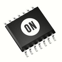
LM2902VDTBG ON Semiconductor, LM2902VDTBG Datasheet - Page 9

LM2902VDTBG
Manufacturer Part Number
LM2902VDTBG
Description
IC OPAMP QUAD SGL SUPPLY 14TSSOP
Manufacturer
ON Semiconductor
Datasheet
1.LM324DR2G.pdf
(15 pages)
Specifications of LM2902VDTBG
Amplifier Type
General Purpose
Number Of Circuits
4
Slew Rate
0.6 V/µs
Gain Bandwidth Product
1MHz
Current - Input Bias
90nA
Voltage - Input Offset
2000µV
Current - Supply
1.4mA
Current - Output / Channel
40mA
Voltage - Supply, Single/dual (±)
3 V ~ 32 V, ±1.5 V ~ 16 V
Operating Temperature
-40°C ~ 125°C
Mounting Type
Surface Mount
Package / Case
14-TSSOP
Number Of Channels
4
Voltage Gain Db
100 dB
Common Mode Rejection Ratio (min)
50 dB
Input Voltage Range (max)
Positive Rail - 5.7 V
Input Voltage Range (min)
Negative Rail
Input Offset Voltage
7 mV
Output Current (typ)
40 mA
Operating Supply Voltage
32 V
Supply Current
1.2 mA
Maximum Operating Temperature
+ 125 C
Mounting Style
SMD/SMT
Maximum Dual Supply Voltage
+/- 16 V
Minimum Operating Temperature
- 40 C
Lead Free Status / RoHS Status
Lead free / RoHS Compliant
Output Type
-
-3db Bandwidth
-
Lead Free Status / Rohs Status
Details
V
V
ref
ref
=
1
2
V
CC
LM324
+
-
1/4
Figure 16. Function Generator
f =
Triangle Wave
C
Output
4 CR
R1 + R
f
R1
R
C
f
75 k
V
if
ref
R3
100 k
R3 =
R1
R2 + R1
R2 R1
LM324
+
-
300 k
R2
1/4
http://onsemi.com
Square
Wave
Output
9
V
in
Figure 17. Multiple Feedback Bandpass Filter
Given: f
Choose value f
Then:
For less than 10% error from operational amplifier,
where f
If source impedance varies, filter may be preceded with
voltage follower buffer to stabilize filter parameters.
R1
A(f
o
o
and BW are expressed in Hz.
o
R3 =
R1 =
R2 =
) = gain at center frequency
R2
= center frequency
C
o
4Q
, C
p f
2 A(f
C
R3
Q
2
o
R1 R3
R1 - R3
C
o
)
R3
V
ref
-
LM324
+
1/4
V
CC
V
ref
=
1
2
V
CC
Q
BW
o
CO = 10 C
C
f
o
O
< 0.1
V
O


