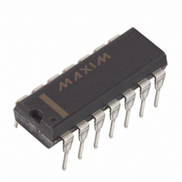
MAX475EPD Maxim Integrated Products, MAX475EPD Datasheet - Page 11

MAX475EPD
Manufacturer Part Number
MAX475EPD
Description
IC OPAMP QUAD 10MHZ 14-DIP
Manufacturer
Maxim Integrated Products
Datasheet
1.MAX475CPD.pdf
(13 pages)
Specifications of MAX475EPD
Amplifier Type
General Purpose
Number Of Circuits
4
Output Type
Rail-to-Rail
Slew Rate
17 V/µs
Gain Bandwidth Product
12MHz
Current - Input Bias
80nA
Voltage - Input Offset
800µV
Current - Supply
2mA
Voltage - Supply, Single/dual (±)
2.7 V ~ 5.25 V, ±1.35 V ~ 2.625 V
Operating Temperature
-40°C ~ 85°C
Mounting Type
Through Hole
Package / Case
14-DIP (0.300", 7.62mm)
Lead Free Status / RoHS Status
Contains lead / RoHS non-compliant
Current - Output / Channel
-
-3db Bandwidth
-
Available stocks
Company
Part Number
Manufacturer
Quantity
Price
Part Number:
MAX475EPD
Manufacturer:
MAXIM/美信
Quantity:
20 000
The MAX473/MAX474/MAX475 have excellent phase
margin (the difference between 180° and the unity-gain
phase angle). It is typically 63° with a load of 10kΩ in
parallel with 20pF. Generally, higher phase margins
indicate greater stability.
Capacitive loads form an RC network with the op amp’s
output resistance, causing additional phase shift that
reduces the phase margin. Figure 3 shows the
MAX473/MAX474/MAX475 output response when dri-
ving a 390pF load in parallel with 10kΩ.
When driving large capacitive loads, add an output iso-
lation resistor, as shown in Figure 4. This resistor
improves the phase margin by isolating the load
capacitance from the amplifier output. Figure 5 shows
the MAX473/MAX474/MAX475 driving a capacitive load
of 1000pF using the circuit of Figure 4.
The feedback resistors appear as a resistance network
to the op amp’s feedback input (Figure 2). This resis-
tance, combined with the op amp’s input and stray
capacitance (total input capacitance), forms a pole that
adds unwanted phase shift when either the total input
capacitance or feedback resistance is too large. For
example, using the noninverting configuration with a
gain of 10, if the total capacitance at the negative input
is 10pF and the effective resistance (R1
this RC network introduces a pole at f
Single/Dual/Quad, 10MHz
Single-Supply Op Amps
Figure 1. Offset Null Circuit
10
______________________________________________________________________________________
4
1
NULL
V
EE
MAX473
Feedback Resistors
2k
NULL
o
8
= 1.8MHz. At
||
R2) is 9kΩ,
input frequencies above f
tional phase shift, which reduces the overall bandwidth
and adversely affects stability. Choose feedback resis-
tors small enough so they do not adversely affect the
op amp’s operation at the frequencies of interest.
The output voltage swing for specified operation is from
(V
Exercising the outputs beyond these limits drives the out-
put transistors toward saturation, resulting in bandwidth
degradation, response-time increase, and gain decrease
(which affects linearity). Operation in this region causes a
slight distortion in the output waveform, but does not
adversely affect the op amp.
Figure 2a. Reducing Offset Error Due to Bias Current:
Inverting Configuration
Figure 2b. Reducing Offset Error Due to Bias Current:
Noninverting Configuration
EE
V
+ 0.3V) to (V
IN
V
R3 = R2 R1
IN
R1
R3
CC
- 0.5V) ( see Electrical Characteristics ).
R3
Overdriving the Outputs
o
, the pole introduces addi-
R2
R3 = R2 R1
R1
R2
V
OUT
V
OUT


