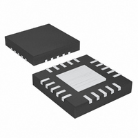
MAX6877ETG+ Maxim Integrated Products, MAX6877ETG+ Datasheet - Page 20

MAX6877ETG+
Manufacturer Part Number
MAX6877ETG+
Description
IC SEQUENCE/SUPERVISOR 24TQFN
Manufacturer
Maxim Integrated Products
Type
Sequencerr
Datasheet
1.MAX6878ETG.pdf
(24 pages)
Specifications of MAX6877ETG+
Number Of Voltages Monitored
3
Output
Open Drain or Open Collector
Reset
Active Low
Reset Timeout
Adjustable/Selectable
Voltage - Threshold
Adjustable/Selectable
Operating Temperature
-40°C ~ 85°C
Mounting Type
Surface Mount
Package / Case
24-TQFN Exposed Pad
Monitored Voltage
- 0.3 V to + 6 V
Manual Reset
Not Resettable
Watchdog
No Watchdog
Supply Voltage (max)
5.5 V
Supply Voltage (min)
2.7 V
Supply Current (typ)
1100 uA
Maximum Power Dissipation
1667 mW
Maximum Operating Temperature
+ 85 C
Mounting Style
SMD/SMT
Minimum Operating Temperature
- 40 C
Lead Free Status / RoHS Status
Lead free / RoHS Compliant
Dual-/Triple-Voltage, Power-Supply
Trackers/Sequencers/Supervisors
When a fault is detected, for a period of t
remains off and the 100Ω pulldowns are turned on.
After the t
retries power-up if all power-up conditions are met (see
Figure 8). These include all V
V
t
When the device is in latch mode and a fault occurs,
FAULT asserts and all outputs are latched off. To
unlatch OUT_ after a fault disappears, cycle EN/UV or
cycle V
threshold. After EN/UV goes high, the device waits a
t
all IN_ are cycled below 2.7V, the device tries to power-
up immediately.
The MAX6877/MAX6878 include a power-good (PG/RST)
output. PG/RST is an open-drain output and requires an
external pullup resistor.
All the OUT_ outputs must exceed their IN_ referenced
thresholds (IN_ x V
period t
tion) before PG/RST asserts high. PG/RST stays low for
the selected reset timeout period (t
the OUT_ voltages exceed their IN_ referenced thresh-
olds. PG/RST goes low when V
V
20
RETRY
RETRY
EN_R
EN_R
______________________________________________________________________________________
MAX6877
MAX6878
MAX6879
, OUT_ voltages < V
, is a function of C
PART
(see Figure 3).
period then tries to power-up again. If V
CC
TIMEOUT
RETRY
and the inputs (IN_) below the 2.7V UVLO
(see the TIMEOUT Period Input sec-
period, the device waits t
TH_PG
Power-Good Output (PG/ RST )
CHANNEL
SLEW
) for the selected reset timeout
TH_PL
3
2
2
; see Table 1.
SET_
SET_
. The autoretry period,
< V
TIMEOUT
> 0.5V, EN/UV >
TH
RETRY
SELECTABLE
or V
TIMEOUT
DELAY
) after all
Yes
Yes
No
, GATE_
EN/UV
CC
and
and
<
The external pass MOSFET is connected in series with
the sequenced power-supply source. Since the load
current and the MOSFET drain-to-source impedance
(R
tics of the MOSFET affect the load supply accuracy.
The MAX6877/MAX6878/MAX6879 fully enhance the
external MOSFET out of its linear range to ensure the
lowest drain-to-source on-impedance. For highest sup-
ply accuracy/lowest voltage drop, select a MOSFET
with an appropriate drain-to-source on-impedance with
a gate-to-source bias of 4.5V to 6.0V.
For better noise immunity, bypass each of the IN_
inputs to GND with 0.1µF capacitors installed as close
to the device as possible. Bypass ABP to GND with a
1µF capacitor installed as close to the device as possi-
ble. ABP is an internally generated voltage and must
not be used to supply power to external circuitry.
DS
PG/RST
) determine the voltage drop, the on characteris-
Yes
Yes
No
Applications Information
MARGIN
Yes
Yes
No
Layout and Bypassing
Selector Guide
MOSFET Selection
V
Yes
Yes
No
CC


