MIC5209-3.3YS Micrel Inc, MIC5209-3.3YS Datasheet - Page 5
MIC5209-3.3YS
Manufacturer Part Number
MIC5209-3.3YS
Description
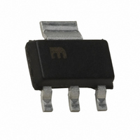
IC REG LDO 500MA 3.3V SOT-223
Manufacturer
Micrel Inc
Datasheet
1.MIC5209-3.3YS_TR.pdf
(13 pages)
Specifications of MIC5209-3.3YS
Regulator Topology
Positive Fixed
Voltage - Output
3.3V
Voltage - Input
Up to 16V
Voltage - Dropout (typical)
0.35V @ 500mA
Number Of Regulators
1
Current - Output
500mA
Operating Temperature
-40°C ~ 125°C
Mounting Type
Surface Mount
Package / Case
SOT-223 (3 leads + Tab), SC-73, TO-261
Output Voltage Fixed
3.3V
Dropout Voltage Vdo
10mV
No. Of Pins
3
Output Current
500mA
Operating Temperature Range
-40°C To +125°C
Msl
MSL 3 - 168 Hours
Termination Type
SMD
Lead Free Status / RoHS Status
Lead free / RoHS Compliant
Current - Limit (min)
-
Lead Free Status / RoHS Status
Lead free / RoHS Compliant, Lead free / RoHS Compliant
Other names
576-3516-5
MIC5209-3.3YS
MIC5209-3.3YS
Available stocks
Company
Part Number
Manufacturer
Quantity
Price
Company:

Part Number:
MIC5209-3.3YS
Manufacturer:
SST
Quantity:
12 600
Part Number:
MIC5209-3.3YS
Manufacturer:
MICREL/麦瑞
Quantity:
20 000
Part Number:
MIC5209-3.3YS TR
Manufacturer:
MICERL
Quantity:
20 000
Part Number:
MIC5209-3.3YSTR
Manufacturer:
MICREL/麦瑞
Quantity:
20 000


ENABLE Input
V
I
I
Notes:
1. Exceeding the absolute maximum rating may damage the device.
2. The device is not guaranteed to function outside its operating rating.
3. The maximum allowable power dissipation at any T
3. The maximum allowable power dissipation at any T
3. The maximum allowable power dissipation at any T (ambient temperature) is calculated using: P
4. Output voltage temperature coeffi cient is the worst case voltage change divided by the total temperature range.
5. Regulation is measured at constant junction temperature using low duty cycle pulse testing. Parts are tested for load regulation in the load range
6. Dropout voltage is defi ned as the input to output differential at which the output voltage drops 2% below its nominal value measured at 1V differen-
7. Ground pin current is the regulator quiescent current plus pass transistor base current. The total current drawn from the supply is the sum of the load
8. V
9. Thermal regulation is the change in output voltage at a time “t” after a change in power dissipation is applied, excluding load or line regulation ef-
10. C
June 2006
ENL
ENL
ENL
ENH
ENL
ENL
ENL
maximum allowable power dissipation will result in excessive die temperature, and the regulator will go into thermal shutdown. See Table 1 and the
“Thermal Considerations” section for details.
“Thermal Considerations” section for details.
“Thermal Considerations”
from 100µA to 500mA. Changes in output voltage due to heating effects are covered by the thermal regulation specifi cation.
tial.
current plus the ground pin current.
fects. Specifi cations are for a 500mA load pulse at V
only].
EN
BYP
is the voltage externally applied to devices with the EN (enable) input pin. [SO-8 (M) and TO-263-5 (U) packages only.]
is an optional, external bypass capacitor connected to devices with a BYP (bypass) or ADJ (adjust) pin. [SO-8 (M) and TO-263-5 (U) packages
Enable Input Logic-Low Voltage
Enable Input Logic-Low Voltage
Enable Input Logic-Low Voltage
Enable Input Logic-Low Voltage
Enable Input Current
Enable Input Current
Enable Input Current
Enable Input Current
A
A
A
A
IN
(ambient temperature) is calculated using: P
= 16V for t = 10ms.
V
V
V
V
V
V
V
V
V
V
V
V
V
V
V
V
V
V
V
V
EN
EN
ENL
ENL
ENL
ENL
ENL
ENL
ENH
ENH
= logic low (regulator shutdown)
= logic low (regulator shutdown)
= logic low (regulator shutdown)
= logic low (regulator shutdown)
= logic low (regulator shutdown)
= logic high (regulator enabled)
= logic high (regulator enabled)
= logic high (regulator enabled)
= logic high (regulator enabled)
= logic high (regulator enabled)
≤ 0.4V
≤ 0.4V
≤ 0.4V
≤ 0.4V
≤ 0.4V
≤ 0.4V
≤ 0.18V
≤ 0.18V
≤ 0.18V
= 2.0V
= 2.0V
= 2.0V
= 2.0V
= 2.0V
= 16V
= 16V
= 16V
= 16V
= 16V
5
D
(max) = (T
J
(max) – T
(max) – T
(max) – T ) ÷ θ
2.0
2.0
2.0
2.0
2.0
A
A
0.01
0.01
0.01
0.01
0.01
0.01
0.01
5
5
5
5
5
JA
. Exceeding the
0.18
0.4
0.4
0.4
0.4
0.4
–1
–1
–1
–1
–1
–1
–2
20
20
20
20
20
25
25
25
25
25
25
30
30
30
30
30
50
M9999-060906
µA
µA
µA
µA
µA
µA
µA
µA
µA
µA
µA
µA
µA
µA
µA
µA
µA
µA
µA
µA
V
V
V
V
V
V
V
V
V
V
V
Related parts for MIC5209-3.3YS
Image
Part Number
Description
Manufacturer
Datasheet
Request
R

Part Number:
Description:
IC REG LDO 500MA 1% 3.6V 8-SOIC
Manufacturer:
Micrel Inc
Datasheet:
Part Number:
Description:
IC REG LDO 500MA 1% 3.0V 8-SOIC
Manufacturer:
Micrel Inc
Datasheet:

Part Number:
Description:
IC REG LDO 500MA 2.5V SOT-223
Manufacturer:
Micrel Inc
Datasheet:
Part Number:
Description:
IC REG LDO 500MA 3.3V LN 8SOIC
Manufacturer:
Micrel Inc
Datasheet:
Part Number:
Description:
IC REG LDO 500MA 1% 2.5V 8-SOIC
Manufacturer:
Micrel Inc
Datasheet:
Part Number:
Description:
IC REG LDO 500MA 1.8V LN 8SOIC
Manufacturer:
Micrel Inc
Datasheet:
Part Number:
Description:
IC REG LDO 500MA 2.5V LN SOT223
Manufacturer:
Micrel Inc
Datasheet:
Part Number:
Description:
IC REG LDO 500MA 3.3V LN 8SOIC
Manufacturer:
Micrel Inc
Datasheet:
Part Number:
Description:
IC REG LDO 500MA 3.3V LN SOT223
Manufacturer:
Micrel Inc
Datasheet:
Part Number:
Description:
IC REG LDO 500MA 5.0V LN SOT223
Manufacturer:
Micrel Inc
Datasheet:

Part Number:
Description:
IC REG LDO 500MA 5.0V LN TO263-5
Manufacturer:
Micrel Inc
Datasheet:
Part Number:
Description:
IC REG LDO 500MA 1% 1.8V TO263-5
Manufacturer:
Micrel Inc
Datasheet:
Part Number:
Description:
IC REG LDO 500MA 1% 2.5V 8-SOIC
Manufacturer:
Micrel Inc
Datasheet:
Part Number:
Description:
IC REG LDO 500MA 1% 2.5V TO263-5
Manufacturer:
Micrel Inc
Datasheet:
Part Number:
Description:
IC REG LDO 500MA 1% 3.0V 8-SOIC
Manufacturer:
Micrel Inc
Datasheet: