NCP699SN50T1G ON Semiconductor, NCP699SN50T1G Datasheet
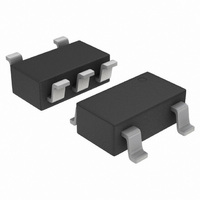
IC REG LDO 150MA 5.0V SOT23-5

NCP699SN50T1G

Manufacturer Part Number
NCP699SN50T1G
Description
IC REG LDO 150MA 5.0V SOT23-5
Manufacturer
ON Semiconductor
Datasheet

Specifications of NCP699SN50T1G

Regulator Topology
Positive Fixed
Voltage - Output
5V
Voltage - Input
Up to 6V
Voltage - Dropout (typical)
0.24V @ 150mA
Number Of Regulators
1
Current - Output
150mA (Min)
Operating Temperature
-40°C ~ 85°C
Mounting Type
Surface Mount
Package / Case
TSOT-23-5, TSOT-5, TSOP-5
Number Of Outputs
1
Polarity
Positive
Input Voltage Max
6 V
Output Voltage
5 V
Output Type
Fixed
Dropout Voltage (max)
0.3 V at 150 mA
Output Current
150 mA
Line Regulation
3 mV / V
Load Regulation
0.8 mV / mA
Voltage Regulation Accuracy
2 %
Maximum Operating Temperature
+ 85 C
Mounting Style
SMD/SMT
Minimum Operating Temperature
- 40 C
Lead Free Status / RoHS Status
Lead free / RoHS Compliant
Current - Limit (min)
-
Lead Free Status / Rohs Status
Lead free / RoHS Compliant
Other names
NCP699SN50T1GOSTR

Available stocks

Company
Part Number
Manufacturer
Quantity
Price
Part Number:
NCP699SN50T1G
Manufacturer:
ON/安森美
Quantity:
20 000
NCP699
150 mA CMOS Low Iq LDO
with Enable in TSOP-5
handheld communication equipment and portable battery powered
applications which require low quiescent current. The NCP699 series
features a very low ground current of 40 mA, independent of load
current. Each device contains a voltage reference unit, an error
amplifier, a PMOS power transistor, internal resistors for setting
output voltage, current limit, and temperature limit protection circuits.
The device is housed in the micro−miniature TSOP−5 surface mount
package. Standard voltage versions are 1.3, 1.4, 1.5, 1.8, 2.5, 2.8, 2.9,
3.0, 3.1, 3.3, 3.4, 4.5 and 5.0 V. Other voltages are available in 100 mV
steps.
Features
Typical Applications
© Semiconductor Components Industries, LLC, 2009
January, 2009 − Rev. 8
The NCP699 series of fixed output LDO’s are designed for
The NCP699 has been designed to be used with low cost capacitors.
Enable Control (Active High, Supports Sub 1 V Logic)
Very Low Ground Current of 40 mA Typical
Low Dropout Voltage of 340 mV at 150 mA, and 3.0 V V
Multiple Fixed Output Voltage Option
Output Voltage Accuracy of 2.0%
Operating Temperature Range of −40°C to 85°C
Stable with 1 mF Ceramic or Tantalum Capacitors
These are Pb−Free Devices
Cellular Phones
Battery Powered Consumer Products
Hand−Held Instruments
Camcorders and Cameras
Printers and Office Equipment
Unregulated
Battery or
Voltage
OFF
ON
Figure 1. Typical Application Diagram
This device contains 86 active transistors
1 mF
C
in
+
1
2
3
5
4
+
C
1 mF
out
Vout
out
1
See detailed ordering and shipping information in the package
dimensions section on page 7 of this data sheet.
5
(Note: Microdot may be in either location)
1
xxx
A
Y
W
G
Enable
ORDERING INFORMATION
Gnd
(SOT23−5, SC59−5)
V
PIN CONNECTIONS
http://onsemi.com
in
SN SUFFIX
= Specific Device Code
= Assembly Location
= Year
= Work Week
= Pb−Free Package
CASE 483
1
2
TSOP−5
3
(Top View)
Publication Order Number:
5
4
5
1
V
N/C
MARKING
DIAGRAM
out
xxx AYWG
NCP699/D
G

Related parts for NCP699SN50T1G

NCP699SN50T1G Summary of contents

Page 1

NCP699 150 mA CMOS Low Iq LDO with Enable in TSOP-5 The NCP699 series of fixed output LDO’s are designed for handheld communication equipment and portable battery powered applications which require low quiescent current. The NCP699 series features a very ...

Page 2

PIN FUNCTION DESCRIPTION Á Á Á Á ...

Page 3

ELECTRICAL CHARACTERISTICS unless otherwise noted.) Characteristic Output Voltage ( mA −40°C to 85°C) out A 1.3 V 1.4 V 1.5 V 1.8 V 2.5 V 2.8 V 2.9 V 3.0 V 3.1 V 3.3 V 3.4 ...

Page 4

T , AMBIENT TEMPERATURE (°C) A Figure 2. Dropout Voltage vs. Temperature −60 −40 −20 ...

Page 5

FREQUENCY (Hz) Figure 8. Output Noise Density Figure 10. Load Transient Response 3.5 3.0 2.5 2.0 1.5 1.0 0 TYPICAL CHARACTERISTICS V = 4.0 V ...

Page 6

Load Regulation The change in output voltage for a change in output current at a constant temperature. Dropout Voltage The input/output differential at which the regulator output no longer maintains regulation against further reductions in input voltage. Measured when the ...

Page 7

... NCP699SN31T1G NCP699SN33T1G NCP699SN34T1G NCP699SN45T1G NCP699SN50T1G *Additional voltages in 100 mV steps are available upon request by contacting your ON Semiconductor representative. †For information on tape and reel specifications, including part orientation and tape sizes, please refer to our Tape and Reel Packaging Specification Brochure, BRD8011/D. APPLICATIONS INFORMATION ...

Page 8

... H T *For additional information on our Pb−Free strategy and soldering details, please download the ON Semiconductor Soldering and Mounting Techniques Reference Manual, SOLDERRM/D. ON Semiconductor and are registered trademarks of Semiconductor Components Industries, LLC (SCILLC). SCILLC reserves the right to make changes without further notice to any products herein. SCILLC makes no warranty, representation or guarantee regarding the suitability of its products for any particular purpose, nor does SCILLC assume any liability arising out of the application or use of any product or circuit, and specifically disclaims any and all liability, including without limitation special, consequential or incidental damages. “ ...

Related keywords