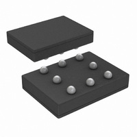
LP2967ITPX-2830/NOPB National Semiconductor, LP2967ITPX-2830/NOPB Datasheet

LP2967ITPX-2830/NOPB
Specifications of LP2967ITPX-2830/NOPB
Related parts for LP2967ITPX-2830/NOPB
LP2967ITPX-2830/NOPB Summary of contents
Page 1
... Multiple voltage options, from 1.8V to 5.0V, are available. Consult factory for custom voltages. Block Diagram © 2005 National Semiconductor Corporation Features n Ultra low drop-out voltage n Guaranteed 150mA output current, 300 mA peak n Smallest possible size (micro SMD package) n Requires minimum external components n Stable with 2.2 µ ...
Page 2
Basic Application Circuit *SD1 and SD2 must be actively terminated. Tie them to V **Minimum capacitance are shown to ensure stability (may be increased without limit). *** Reduces output noise (may be omitted if application is not noise critical). Use ...
Page 3
... For 8-Bump micro SMD Package (TPA08) 1.8 2.5 STD 1.8 2.5 STD Package Order Information Marking LP2967IBP-2833 CC LP2967IBPX-2833 CC LP2967ITP-1825 L07 LP2967ITPX-1825 L07 3 Supplied As 1000 Units Tape and Reel 3500 Units Tape and Reel 1000 Units Tape and Reel 3500 Units Tape and Reel 10114205 10114206 www.national.com ...
Page 4
Package Outline and Connection Diagram Top View micro SMD 8-Bump micro SMD Package Code: BP, TP Pin Description Pin Number Name micro SMD OUT SD2 B1 BYPASS C1 GND C2 GND C3 SD1 ...
Page 5
... Absolute Maximum Ratings If Military/Aerospace specified devices are required, please contact the National Semiconductor Sales Office/ Distributors for availability and specifications. Storage Temperature Range Lead Temp reflow, 10 sec.) Pad Temp. (IR reflow, 10 sec.) Operating Junction Temp. Range Power Dissipation (Note 4) Electrical Characteristics Limits in standard typeface are for T j range ...
Page 6
Electrical Characteristics Limits in standard typeface are for T range. Unless otherwise specified, V Symbol Parameter RR Ripple Rejection Crosstalk Xtalk Rejection Note 1: Absolute maximum ratings indicate limits beyond which damage to the device may occur. Electrical specifications do ...
Page 7
Typical Performance Characteristics = 1.6V 1mA 25˚ Output Voltage vs Temperature Output Voltage vs Temperature Dropout Voltage vs Temp. and Load Unless otherwise specified: C Output Voltage vs Temperature 10114255 Dropout Voltage vs Load ...
Page 8
Typical Performance Characteristics = 1.6V 1mA 25˚C. (Continued Cross Channel Isolation OUT OUT Input Current vs V Input Current www.national.com Unless otherwise ...
Page 9
Typical Performance Characteristics = 1.6V 1mA 25˚C. (Continued Short Circuit Current vs V Short Circuit Current Line Transient Reponse Unless otherwise specified: C Short Circuit Current vs Time OUT 10114258 10114260 10114223 9 = ...
Page 10
Typical Performance Characteristics = 1.6V 1mA 25˚C. (Continued Load Transient Reponse (V Load Transient Reponse (V Load Transient Reponse (V www.national.com Unless otherwise specified Load Transient Reponse (V OUT 10114231 1) Load ...
Page 11
Typical Performance Characteristics = 1.6V 1mA 25˚C. (Continued LP2967-2.5V Turn-On Time (2nd Output OFF) Output Impedance vs Frequency Ripple Rejection vs Frequency Unless otherwise specified: C LP2967-2.5V Turn-On Time (2nd Output ON) 10114240 Ripple ...
Page 12
Typical Performance Characteristics = 1.6V 1mA 25˚C. (Continued Ripple Rejection vs Frequency Ripple Rejection vs Frequency Output Noise Density www.national.com Unless otherwise specified: C Ripple Rejection vs Frequency 10114252 Output Noise Density 10114254 10114261 ...
Page 13
Application Hints EXTERNAL CAPACITORS The LP2967 low dropout regulator requires two external capacitors, C and C to assure the device’s output IN OUT stability. C may be used to reduce output noise. The BYPASS capacitors must be correctly selected with ...
Page 14
Application Hints (Continued) LP2967-2.5V Region Of Stability with 2.2 µF C No-Load Operation If a 2.2 µF output capacitor is used, the minimum stable ESR value rises to about 0.5 Ω at load currents below 1 mA. If < the ...
Page 15
Application Hints (Continued) MAXIMUM POWER DISSAIPATION CAPABILITY Each output pin the LP2967 can deliver a current 150mA over the full operating junction temperature range. However, the maximum output current must be derated at higher ambient temperature to ...
Page 16
Physical Dimensions www.national.com inches (millimeters) unless otherwise noted micro SMD Package NS Package Number TPA08F5A The dimensions of X1, X2, and X3 are given below 1.412mm X2 = 1.946mm X3 = 0.500mm 16 ...
Page 17
Physical Dimensions inches (millimeters) unless otherwise noted (Continued) The dimensions of X1, X2, and X3 are given below: For Ordering, Refer to Ordering Information Table micro SMD Package NS Package Number BPA08F5B X1 = 1.412mm X2 = 1.946mm X3 = ...
Page 18
... BANNED SUBSTANCE COMPLIANCE National Semiconductor manufactures products and uses packing materials that meet the provisions of the Customer Products Stewardship Specification (CSP-9-111C2) and the Banned Substances and Materials of Interest Specification (CSP-9-111S2) and contain no ‘‘Banned Substances’’ as defined in CSP-9-111S2. ...


