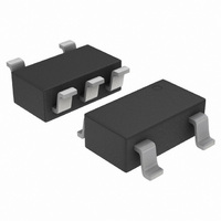
NCV8560SN500T1G ON Semiconductor, NCV8560SN500T1G Datasheet

NCV8560SN500T1G
Specifications of NCV8560SN500T1G
Available stocks
Related parts for NCV8560SN500T1G
NCV8560SN500T1G Summary of contents
Page 1
NCV8560 High Performance Low-Power, LDO Regulator with Enable The NCV8560 provides 150 mA of output current at fixed voltage options adjustable output voltage from 5.0 V down to 1.250 designed for portable battery powered applications ...
Page 2
GND ENABLE 3 4 (Top View) * ADJ − Adjustable Version * NC − Fixed Voltage Version Figure 2. Pin Connections − TSOP5 PIN FUNCTION DESCRIPTION Pin No. Á Á Á Á DFN6 TSOP−5 Pin ...
Page 3
ELECTRICAL CHARACTERISTICS (V = 1.750 1.250 out in out Characteristic Regulator Output (Adjustable Voltage Version) Output Voltage Ripple Rejection ( out + 1 0 p−p ...
Page 4
ELECTRICAL CHARACTERISTICS =1.0 mF, −40°C ≤ T ≤ 125°C, Figure 4, unless otherwise specified.) (Note 10) in out A Characteristic General Disable Current Ground Current Adjustable Option 1.3 V Option 1.5 V Option 1 3.0 ...
Page 5
OUT IN NCV8560 (adjustable ADJ GND Figure 4. Typical Application Circuit for V (Adjustable Version OUT IN NCV8560 (adjustable ADJ GND Figure 5. Typical Application Circuit ...
Page 6
I = 1.0 mA out 1.252 I = 150 mA out 1.248 1.244 1.240 −40 − AMBIENT TEMPERATURE (°C) A Figure 7. Output Voltage vs. Temperature ( 0.5 V) ...
Page 7
I out 4.995 4.990 I out 4.985 4.980 4.975 4.970 4.965 −40 − AMBIENT TEMPERATURE (°C) A Figure 13. Output Voltage vs. Temperature (5.0 V Fixed Output, V 250 V = ADJ out I ...
Page 8
T , AMBIENT TEMPERATURE (°C) A Figure 19. Ground Current (Sleep Mode) vs. Temperature 160 3.0 V 2.8 V 140 1.5 V 3.3 V 120 1.8 V 100 ...
Page 9
T , AMBIENT TEMPERATURE (°C) A Figure 24. Output Short Circuit Current vs. Temperature 4.0 3.0 2 out ...
Page 10
TYPICAL CHARACTERISTICS 5.0 V out V = 1.25 V out 1.0 Stable Region 0.1 C out T = −40°C to 125° 6 0. OUTPUT ...
Page 11
Load Regulation The change in output voltage for a change in output load current at a constant temperature. Dropout Voltage The input/output differential at which the regulator output no longer maintains regulation against further reductions in input voltage. Measured when ...
Page 12
Noise Decoupling The NCV8560 is a low noise regulator and needs no external noise reduction capacitor. Unlike other low noise regulators which require an external capacitor and have slow startup times, the NCV8560 operates without a noise reduction capacitor, has ...
Page 13
... NCV8560SN130T1G NCV8560SN150T1G NCV8560SN180T1G NCV8560SN250T1G NCV8560SN280T1G NCV8560SN300T1G NCV8560SN330T1G NCV8560SN350T1G NCV8560SN500T1G *For additional information on our Pb−Free strategy and soldering details, please download the ON Semiconductor Soldering and Mounting Techniques Reference Manual, SOLDERRM/D. Marking Code Version 1st Line: V8560 ADJ 2nd Line: ADJ 1st Line: V8560 1 ...
Page 14
D PIN ONE REFERENCE 2X 0.15 C TOP VIEW 2X 0.15 C DETAIL B 0.10 C Ç Ç Ç Ç Ç Ç 6X 0.08 C Ç Ç Ç (A3) A1 SEATING PLANE SIDE VIEW D2 Ç Ç Ç Ç 1 ...
Page 15
... H T *For additional information on our Pb−Free strategy and soldering details, please download the ON Semiconductor Soldering and Mounting Techniques Reference Manual, SOLDERRM/D. ON Semiconductor and are registered trademarks of Semiconductor Components Industries, LLC (SCILLC). SCILLC reserves the right to make changes without further notice to any products herein. SCILLC makes no warranty, representation or guarantee regarding the suitability of its products for any particular purpose, nor does SCILLC assume any liability arising out of the application or use of any product or circuit, and specifically disclaims any and all liability, including without limitation special, consequential or incidental damages. “ ...


