TC55RP3002EMB713 Microchip Technology, TC55RP3002EMB713 Datasheet - Page 9
TC55RP3002EMB713
Manufacturer Part Number
TC55RP3002EMB713
Description
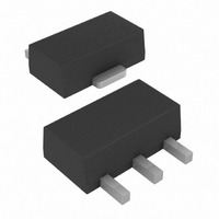
IC REG LDO 3.0V 150MA SOT-89-3
Manufacturer
Microchip Technology
Datasheet
1.TC55RP5002EZB.pdf
(18 pages)
Specifications of TC55RP3002EMB713
Regulator Topology
Positive Fixed
Voltage - Output
3V
Voltage - Input
Up to 10V
Number Of Regulators
1
Current - Output
150mA (Min)
Operating Temperature
-40°C ~ 85°C
Mounting Type
Surface Mount
Package / Case
SC-62, SOT-89, TO-243 (3 Leads + Tab)
Lead Free Status / RoHS Status
Request inventory verification / Request inventory verification
Voltage - Dropout (typical)
-
Current - Limit (min)
-
Other names
158-2042-2
158-2042-2
TC55RP3002EMB71TR
158-2042-2
TC55RP3002EMB71TR
Available stocks
Company
Part Number
Manufacturer
Quantity
Price

Part Number:
TC55RP3002EMB713
Manufacturer:
MICROCHI
Quantity:
20 000


3.0
The descriptions of the pins are listed in Table 3-1.
TABLE 3-1:
3.1
Regulator ground. Tie GND to the negative side of the
output and the negative side of the input capacitor.
Only the LDO bias current (1 µA typical) flows out of
this pin, there is no high current. The LDO output regu-
lation is referenced to this pin. Minimize voltage drops
between this pin and the minus side of the load.
3.2
Connect V
positive terminal of the output capacitor. The positive
side of the output capacitor should be physically
located as close to the LDO V
The current flowing out of this pin is equal to the DC
load current.
3.3
Connect the input supply voltage and the positive side
of the input capacitor to V
be physically located as close as is practical to V
current flow into this pin is equal to the DC load current,
plus the LDO bias current (1 µA typical.)
© 2005 Microchip Technology Inc.
1
2
3
Pin No.
PIN DESCRIPTIONS
Ground Terminal (GND)
Regulated Voltage Output (V
Unregulated Supply Input (V
OUT
Symbol
V
GND
V
to the positive side of the load and the
OUT
IN
PIN FUNCTION TABLE
Ground Terminal
Regulated Voltage Output
Unregulated Supply Input
IN
. The input capacitor should
OUT
Description
pin as is practical.
IN
OUT
IN
)
. The
)
4.0
The TC55 is a low quiescent current, precision, fixed-
output voltage LDO. Unlike bipolar regulators, the
TC55 supply current does not increase proportionally
with load current.
4.1
A minimum of 1 µF output capacitor is required. The
output capacitor should have an effective series resis-
tance (esr) greater than 0.1
resonant frequency above 1 MHz. Larger output
capacitors can be used to improve supply noise rejec-
tion and transient response. Care should be taken
when increasing C
ance is not high enough to cause high input impedance
oscillation.
4.2
A 1 µF input capacitor is recommended for most
applications when the input impedance is on the order
of 10 . Larger input capacitance may be required for
stability when operating off of a battery input, or if there
is a large distance from the input source to the LDO.
When large values of output capacitance are used, the
input capacitance should be increased to prevent high
source impedance oscillations.
DETAILED DESCRIPTION
Output Capacitor
Input Capacitor
OUT
to ensure that the input imped-
and less than 5 , plus a
DS21435F-page 9
TC55
Related parts for TC55RP3002EMB713
Image
Part Number
Description
Manufacturer
Datasheet
Request
R

Part Number:
Description:
Manufacturer:
Microchip Technology Inc.
Datasheet:
Part Number:
Description:
Manufacturer:
Microchip Technology Inc.
Datasheet:
Part Number:
Description:
Manufacturer:
Microchip Technology Inc.
Datasheet:
Part Number:
Description:
Manufacturer:
Microchip Technology Inc.
Datasheet:
Part Number:
Description:
Manufacturer:
Microchip Technology Inc.
Datasheet:
Part Number:
Description:
Manufacturer:
Microchip Technology Inc.
Datasheet:
Part Number:
Description:
Manufacturer:
Microchip Technology Inc.
Datasheet:
Part Number:
Description:
Manufacturer:
Microchip Technology Inc.
Datasheet: