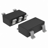
NCP361SNT1G ON Semiconductor, NCP361SNT1G Datasheet - Page 2

NCP361SNT1G
Manufacturer Part Number
NCP361SNT1G
Description
IC USB POS OVP/OCP SOT23-5
Manufacturer
ON Semiconductor
Datasheet
1.NCP361SNT1G.pdf
(12 pages)
Specifications of NCP361SNT1G
Voltage - Working
1.2 ~ 20V
Technology
Mixed Technology
Number Of Circuits
1
Applications
General Purpose
Package / Case
TSOT-23-5, TSOT-5, TSOP-5
Voltage Supervisor Type
Voltage Detector
Number Of Voltage Supervisors
1
Reset Threshold Voltage (min)
5.43V
Reset Threshold Voltage (max)
5.9V
Operating Supply Voltage (min)
1.2V
Operating Supply Voltage (max)
20V
Package Type
TSOP
Operating Temperature Classification
Industrial
Operating Temp Range
-40C to 85C
Pin Count
5
Mounting
Surface Mount
Number Of Voltages Monitored
1
Monitored Voltage
20 V
Undervoltage Threshold
3 V
Overvoltage Threshold
5.675 V
Output Type
PFET Driver
Manual Reset
Not Resettable
Watchdog
No Watchdog
Supply Voltage (max)
20 V
Supply Voltage (min)
1.2 V
Maximum Operating Temperature
+ 85 C
Mounting Style
SMD/SMT
Minimum Operating Temperature
- 40 C
Lead Free Status / RoHS Status
Lead free / RoHS Compliant
Power (watts)
-
Voltage - Clamping
-
Lead Free Status / Rohs Status
Compliant
Other names
NCP361SNT1GOSTR
Available stocks
Company
Part Number
Manufacturer
Quantity
Price
Company:
Part Number:
NCP361SNT1G
Manufacturer:
TOREX
Quantity:
12 000
Part Number:
NCP361SNT1G
Manufacturer:
ON/安森美
Quantity:
20 000
NOTE:
PIN FUNCTION DESCRIPTION (UDFN Package)
PIN FUNCTION DESCRIPTION (TSOP−5 Package)
Pin No.
Pin No.
INPUT
4, 5
1
2
3
6
1
2
3
4
5
EN
Pin out provided for concept purpose only and might change in the final product
Name
FLAG
Name
FLAG
GND
OUT
GND
OUT
EN
EN
IN
IN
1 mF 25 V X5R 0603
OUTPUT
OUTPUT
OUTPUT
OUTPUT
POWER
POWER
POWER
POWER
INPUT
INPUT
Type
Type
LDO
Enable Pin. The device enters in shutdown mode when this pin is tied to a high level. In this case the
output is disconnected from the input. To allow normal functionality, the EN pin shall be connected to
GND or to a I/O pin. This pin does not have an impact on the fault detection.
Ground
Input Voltage Pin. This pin is connected to the VBUS. A 1 mF low ESR ceramic capacitor, or larger,
must be connected between this pin and GND.
Output Voltage Pin. The output is disconnected from the VBUS power supply when the input voltage is
above OVLO threshold or below UVLO threshold. A 1 mF capacitor must be connected to these pins.
The two OUT pins must be hardwired to common supply.
Fault Indication Pin. This pin allows an external system to detect a fault on VBUS pin. The FLAG pin
goes low when input voltage exceeds OVLO threshold. Since the FLAG pin is open drain functionality,
an external pull up resistor to V
Input Voltage Pin. This pin is connected to the VBUS. A 1 mF low ESR ceramic capacitor, or larger,
must be connected between this pin and GND.
Ground
Enable Pin. The device enters in shutdown mode when this pin is tied to a high level. In this case the
output is disconnected from the input. To allow normal functionality, the EN pin shall be connected to
GND or to a I/O pin. This pin does not have an impact on the fault detection.
Fault Indication Pin. This pin allows an external system to detect a fault on VBUS pin. The FLAG pin
goes low when input voltage exceeds OVLO threshold. Since the FLAG pin is open drain functionality,
an external pull up resistor to V
Output Voltage Pin. The output is disconnected from the VBUS power supply when the input voltage is
above OVLO threshold or below UVLO threshold. A 1 mF capacitor must be connected to this pin.
INPUT
Figure 1. Typical Application Circuit (UDFN Pinout)
C1
Thermal Shutdown
Figure 2. Functional Block Diagram
1
3
V
EN
REF
IN
NCP361
GND
2
http://onsemi.com
FLAG
OUT
OUT
CC
CC
4
5
6
2
must be added.
must be added.
C2
OUTPUT
Soft Start
OVLO
UVLO
1 mF 25 V X5R 0603
Description
Description
FLAG
FLAG Power
FLAG_State
2
1
R1
1M
J2
FLAGV
OUTPUT
(2 out pins in
UDFN package)


