STN4NF20L STMicroelectronics, STN4NF20L Datasheet
STN4NF20L
Specifications of STN4NF20L
Available stocks


Related parts for STN4NF20L


STN4NF20L Summary of contents
Page 1
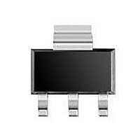
... Device summary Order code STN4NF20L October 2010 N-channel 200 V, 1.1 Ω SOT-223 low gate charge STripFET™ II Power MOSFET R DS(on max. < 1.5 Ω Figure 1. Marking 4NF20L Doc ID 17445 Rev 2 STN4NF20L SOT-223 Internal schematic diagram Package Packaging SOT-223 Tape and reel 1/12 www.st.com 12 ...
Page 2
... Contents Contents 1 Electrical ratings . . . . . . . . . . . . . . . . . . . . . . . . . . . . . . . . . . . . . . . . . . . . 3 2 Electrical characteristics . . . . . . . . . . . . . . . . . . . . . . . . . . . . . . . . . . . . . 4 2.1 Electrical characteristics (curves) 3 Test circuits 4 Package mechanical data . . . . . . . . . . . . . . . . . . . . . . . . . . . . . . . . . . . . . 9 5 Revision history . . . . . . . . . . . . . . . . . . . . . . . . . . . . . . . . . . . . . . . . . . . 11 2/ Doc ID 17445 Rev 2 STN4NF20L ...
Page 3
... STN4NF20L 1 Electrical ratings Table 2. Absolute maximum ratings Symbol V Gate-source voltage GS I Drain current continuous Drain current continuous T D (1) I Drain current pulsed DM (2) P Total dissipation at T TOT (3) dv/dt Peak diode recovery voltage slope T Operating junction temperature j T Storage temperature stg 1. Pulse width limited by safe operating area. ...
Page 4
... Figure 12) Doc ID 17445 Rev 2 Min. Typ 200 =125 ° 0.5 A 1.1 1.13 Min. Typ. 150 - 5 0.9 - 2.6 6.9 Min. Typ. 3 10.4 15.4 STN4NF20L Max. Unit V 1 µA 50 µA ± 100 Ω 1.5 Ω 1.55 Max. Unit Ω Max Unit ...
Page 5
... STN4NF20L Table 8. Source drain diode Symbol Source-drain current I SD Source-drain current (1) I SDM (pulsed) (2) V Forward on voltage SD t Reverse recovery time rr Q Reverse recovery charge rr I Reverse recovery current RRM t Reverse recovery time rr Q Reverse recovery charge rr I Reverse recovery current RRM 1 ...
Page 6
... V (V) 100 DS Figure 5. AM08186v1 temperature Figure 7. AM08188v1 R DS(on) (Ohm) 1.08 1.06 1.04 1. (°C) 100 J Doc ID 17445 Rev 2 STN4NF20L Thermal impedance Transfer characteristics V =15V Static drain-source on resistance I =0. = =10V GS 1 0.2 0.4 0.6 0.8 0 AM08187v1 9 V (V) GS AM08189v1 1 I (A) ...
Page 7
... STN4NF20L Figure 8. Gate charge vs gate-source voltage Figure (V) V =160V = Figure 10. Normalized gate threshold voltage vs temperature V GS(th) (norm) 1.10 1.00 0.90 0.80 0.70 -50 - AM08190v1 C (pF 300 500 400 200 300 200 100 100 (nC) g Figure 11. Normalized on resistance vs AM08192v1 R DS(on) (norm) 2.1 1.9 1 ...
Page 8
... AM01468v1 Figure 15. Unclamped inductive load test 3.3 1000 μF μ AM01470v1 Figure 17. Switching time waveform V (BR)DSS 10% 0 AM01472v1 Doc ID 17445 Rev 2 STN4NF20L 12V 47kΩ 100nF I =CONST G 100Ω GMAX 2200 μF 2.7kΩ 47kΩ 1kΩ circuit 2200 3.3 μ ...
Page 9
... STN4NF20L 4 Package mechanical data In order to meet environmental requirements, ST offers these devices in different grades of ® ECOPACK packages, depending on their level of environmental compliance. ECOPACK specifications, grade definitions and product status are available at: www.st.com. ECOPACK trademark. Doc ID 17445 Rev 2 Package mechanical data ® 9/12 ...
Page 10
... Package mechanical data DIM 10/12 SOT-223 mechanical data mm. min. typ 0.02 0.60 0.70 2.90 3.00 0.24 0.26 6.30 6.50 2.30 4.60 3.30 3.50 6.70 7.00 Doc ID 17445 Rev 2 STN4NF20L max. 1.80 0.1 0.85 3.15 0.35 6.70 3.70 7. 0046067_L ...
Page 11
... STN4NF20L 5 Revision history Table 9. Document revision history Date 29-Apr-2010 11-Oct-2010 Revision 1 First release. 2 Document status promoted from preliminary data to datasheet. Doc ID 17445 Rev 2 Revision history Changes 11/12 ...
Page 12
... Australia - Belgium - Brazil - Canada - China - Czech Republic - Finland - France - Germany - Hong Kong - India - Israel - Italy - Japan - Malaysia - Malta - Morocco - Philippines - Singapore - Spain - Sweden - Switzerland - United Kingdom - United States of America 12/12 Please Read Carefully: © 2010 STMicroelectronics - All rights reserved STMicroelectronics group of companies www.st.com Doc ID 17445 Rev 2 STN4NF20L ...