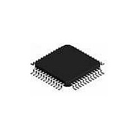
MC68908GZ8MFAE Freescale Semiconductor, MC68908GZ8MFAE Datasheet - Page 214

MC68908GZ8MFAE
Manufacturer Part Number
MC68908GZ8MFAE
Description
IC MCU 8BIT 8K FLASH 48-LQFP
Manufacturer
Freescale Semiconductor
Series
HC08r
Datasheet
1.MC68908GZ8CFJER.pdf
(314 pages)
Specifications of MC68908GZ8MFAE
Core Processor
HC08
Core Size
8-Bit
Speed
8MHz
Connectivity
CAN, LIN, SCI, SPI
Peripherals
LVD, POR, PWM
Number Of I /o
37
Program Memory Size
8KB (8K x 8)
Program Memory Type
FLASH
Ram Size
1K x 8
Voltage - Supply (vcc/vdd)
3 V ~ 5.5 V
Data Converters
A/D 8x10b
Oscillator Type
Internal
Operating Temperature
-40°C ~ 125°C
Package / Case
48-LQFP
Processor Series
M689xx
Core
HC08
Data Bus Width
8 bit
Data Ram Size
1 KB
Interface Type
SPI, SCI, CAN
Maximum Clock Frequency
8 MHz
Number Of Programmable I/os
37
Number Of Timers
2
Operating Supply Voltage
5.5 V
Maximum Operating Temperature
+ 125 C
Mounting Style
SMD/SMT
Development Tools By Supplier
FSICEBASE, M68CBL05AE, DEMO908GZ60E, M68EML08GZE
Minimum Operating Temperature
- 40 C
On-chip Adc
10 bit, 16 Channel
Lead Free Status / RoHS Status
Lead free / RoHS Compliant
Eeprom Size
-
Lead Free Status / Rohs Status
Details
- Current page: 214 of 314
- Download datasheet (5Mb)
System Integration Module (SIM)
The SIM is responsible for:
Table 16-1
214
Addr.
$FE00
$FE01
$FE03
$FE04
$FE05
$FE06
Signal Name
•
•
•
•
•
CGMXCLK
CGMVCLK
CGMOUT
PORRST
IRST
R/W
IAB
IDB
Bus clock generation and control for CPU and peripherals:
–
–
Master reset control, including power-on reset (POR) and computer operating properly (COP)
timeout
Interrupt control:
–
–
–
CPU enable/disable timing
Modular architecture expandable to 128 interrupt sources
Stop/wait/reset/break entry and recovery
Internal clock control
Acknowledge timing
Arbitration control timing
Vector address generation
SIM Break Flag Control
Register Name
shows the internal signal names used in this section.
Register (SBFCR)
SIM Break Status
SIM Reset Status
Register 1 (INT1)
Register 2 (INT2)
Register 3 (INT3)
Register (SBSR)
Register (SRSR)
Interrupt Status
Interrupt Status
Interrupt Status
See page 228.
See page 228.
See page 229.
See page 224.
See page 224.
See page 224.
Buffered version of OSC1 from clock generator module (CGM)
PLL output
PLL-based or OSC1-based clock output from CGM module (Bus clock = CGMOUT divided by two)
Internal address bus
Internal data bus
Internal reset signal
Read/write signal
Signal from the power-on reset module to the SIM
Reset:
Reset:
Reset:
Reset:
Reset:
MC68HC908GZ16 • MC68HC908GZ8 Data Sheet, Rev. 4
Read:
Read:
Read:
Read:
Read:
Read:
Write:
Write:
Write:
Write:
Write:
Write:
POR:
Figure 16-2. SIM I/O Register Summary
Table 16-1. Signal Name Conventions
1. Writing a logic 0 clears SBSW.
BCFE
Bit 7
POR
IF14
IF6
R
R
R
R
0
1
0
0
0
0
0
= Unimplemented
IF13
PIN
IF5
R
R
R
R
R
6
0
0
0
0
0
0
COP
IF12
IF20
IF4
R
R
R
R
R
5
0
0
0
0
0
Description
ILOP
IF11
IF19
IF3
R
R
R
R
R
R
4
0
0
0
0
0
= Reserved
ILAD
IF10
IF18
IF2
R
R
R
R
R
3
0
0
0
0
0
MODRST
IF17
IF1
IF9
R
R
R
R
R
2
0
0
0
0
0
Freescale Semiconductor
Note
SBSW
IF16
LVI
IF8
R
R
R
R
1
0
0
0
0
0
0
(1)
Bit 0
IF15
IF7
R
R
R
R
R
0
0
0
0
0
0
0
Related parts for MC68908GZ8MFAE
Image
Part Number
Description
Manufacturer
Datasheet
Request
R
Part Number:
Description:
Manufacturer:
Freescale Semiconductor, Inc
Datasheet:
Part Number:
Description:
Manufacturer:
Freescale Semiconductor, Inc
Datasheet:
Part Number:
Description:
Manufacturer:
Freescale Semiconductor, Inc
Datasheet:
Part Number:
Description:
Manufacturer:
Freescale Semiconductor, Inc
Datasheet:
Part Number:
Description:
Manufacturer:
Freescale Semiconductor, Inc
Datasheet:
Part Number:
Description:
Manufacturer:
Freescale Semiconductor, Inc
Datasheet:
Part Number:
Description:
Manufacturer:
Freescale Semiconductor, Inc
Datasheet:
Part Number:
Description:
Manufacturer:
Freescale Semiconductor, Inc
Datasheet:
Part Number:
Description:
Manufacturer:
Freescale Semiconductor, Inc
Datasheet:
Part Number:
Description:
Manufacturer:
Freescale Semiconductor, Inc
Datasheet:
Part Number:
Description:
Manufacturer:
Freescale Semiconductor, Inc
Datasheet:
Part Number:
Description:
Manufacturer:
Freescale Semiconductor, Inc
Datasheet:
Part Number:
Description:
Manufacturer:
Freescale Semiconductor, Inc
Datasheet:
Part Number:
Description:
Manufacturer:
Freescale Semiconductor, Inc
Datasheet:
Part Number:
Description:
Manufacturer:
Freescale Semiconductor, Inc
Datasheet:


