ST16C550IJ44-F Exar Corporation, ST16C550IJ44-F Datasheet
ST16C550IJ44-F
Specifications of ST16C550IJ44-F
Available stocks


Related parts for ST16C550IJ44-F

ST16C550IJ44-F Summary of contents
Page 1
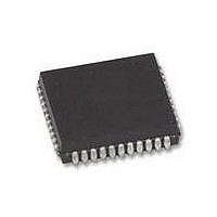
... Four selectable receive FIFO interrupt trigger levels ORDERING INFORMATION Part number Package ST16C550CP40 40-Lead PDIP ST16C550CJ44 44-Lead PLCC ST16C550CQ48 48-Lead TQFP ST16C550IP40 40-Lead PDIP ST16C550IJ44 44-Lead PLCC ST16C550IQ48 48-Lead TQFP Rev. 5.01 EXAR Corporation, 48720 Kato Road, Fremont, CA 94538 (510) 668-7000 FAX (510) 668-7017 ...
Page 2
ST16C550 Figure 1, PACKAGE DESCRIPTION, ST16C550 48 Pin TQFP Package 1 N. RCLK N.C. 6 ST16C550CQ48 CS0 9 CS1 10 -CS2 11 -BAUDOUT 12 Rev. 5.01 40 Pin DIP ...
Page 3
Figure 2, BLOCK DIAGRAM D0-D7 -IOR,IOR -IOW,IOW RESET A0-A2 -AS CS0,CS1 -CS2 -DDIS INT -RXRDY -TXRDY Rev. 5.01 ST16C550 Transmit Transmit FIFO Shift Registers Register Receive Receive FIFO Shift Registers Register Modem Control Clock Logic & Baud Rate Generator 3 ...
Page 4
ST16C550 SYMBOL DESCRIPTION Symbol Pin IOR 22 25 CS0 12 14 CS1 13 15 -CS2 14 16 IOW D0-D7 1-8 2-9 GND 20 22 ...
Page 5
SYMBOL DESCRIPTION Symbol Pin 40 44 -IOR 21 24 -IOW 18 20 INT 30 33 -RXRDY 29 32 -TXRDY 24 27 -BAUDOUT 15 17 Rev. 5.01 Signal Pin Description 48 type 19 I Read data strobe (active low strobe). A ...
Page 6
ST16C550 SYMBOL DESCRIPTION Symbol Pin 40 44 -DDIS 23 26 -OP1 34 38 RESET 35 39 RCLK 9 10 -OP2 31 35 VCC 40 44 XTAL1 16 18 XTAL2 Rev. 5.01 Signal Pin Description 48 ...
Page 7
SYMBOL DESCRIPTION Symbol Pin 40 44 -CTS 36 40 -DSR 37 41 -DTR -RTS Rev. 5.01 Signal 48 type 38 I Clear to Send (active low) - ...
Page 8
ST16C550 GENERAL DESCRIPTION The ST16C550 provides serial asynchronous receive data synchronization, parallel-to-serial and serial-to- parallel data conversions for both the transmitter and receiver sections. These functions are necessary for converting the serial data stream into parallel data that is required ...
Page 9
Table 2, INTERNAL REGISTER DECODE READ MODE General Register Set (THR/RHR, IER/ISR, MCR/MSR, LCR/LSR, SPR Receive Holding Register Interrupt Enable Register Interrupt Status Register Line ...
Page 10
ST16C550 ample [(programmed word length = 7) + (stop bit = 1) + (start bit = 1) = 9]. 40 (bit times divided 4.4 characters. Example -B: If the user programs the word length = ...
Page 11
DMA Operation The ST16C550 FIFO trigger level provides additional flexibility to the user for block mode operation. The user can optionally operate the transmit and receive FIFO’s in the DMA mode (FCR bit-3). The DMA mode affects the state of ...
Page 12
ST16C550 Figure 4, INTERNAL LOOP-BACK MODE DIAGRAM D0-D7 -IOR,IOR -IOW,IOW RESET A0-A2 -AS CS0,CS1 -CS2 -DDIS INT -TXRDY -RXRDY Rev. 5.01 Transmit Transmit FIFO Shift Registers Register Receive Receive FIFO Shift Registers Register Clock & Baud Rate Generator 12 VCC ...
Page 13
REGISTER FUNCTIONAL DESCRIPTIONS The following table delineates the assigned bit functions for the twelve ST16C550 internal registers. The assigned bit functions are more fully defined in the following paragraphs. Table 4, ST16C550 INTERNAL REGISTERS Register BIT-7 [Default] ...
Page 14
ST16C550 Transmit and Receive Holding Register The serial transmitter section consists of an 8-bit Transmit Hold Register (THR) and Transmit Shift Register (TSR). The status of the THR is provided in the Line Status Register (LSR). Writing to the THR ...
Page 15
IER BIT-3: Logic 0 = Disable the modem status register interrupt. (normal default condition) Logic 1 = Enable the modem status register interrupt. IER BIT 4-7: Not used and set to “0”. FIFO Control Register (FCR) This register is used ...
Page 16
ST16C550 Interrupt Status Register (ISR) The ST16C550 provides four levels of prioritized inter- rupts to minimize external software interaction. The Interrupt Status Register (ISR) provides the user with six interrupt status bits. Performing a read cycle on the ISR will ...
Page 17
ISR BIT-0: Logic interrupt is pending and the ISR contents may be used as a pointer to the appropriate interrupt service routine. Logic interrupt pending. (normal default condi- tion) ISR BIT 1-3: (logic 0 ...
Page 18
ST16C550 LCR BIT-6: When enabled the Break control bit causes a break condition to be transmitted (the TX output is forced to a logic 0 state). This condition exists until disabled by setting LCR bit logic 0. Logic ...
Page 19
UART to issue an interrupt to CPU when the THR interrupt enable is set. The THR bit is set to a logic 1 when a character is transferred from the transmit holding register into the transmitter ...
Page 20
ST16C550 ST16C550 EXTERNAL RESET CONDITIONS REGISTERS RESET STATE IER IER BITS 0-7 = logic 0 ISR ISR BIT-0=1, ISR BITS 1-7 = logic 0 LCR, MCR BITS 0-7 = logic 0 LSR LSR BITS 0-4 = logic 0, LSR BITS ...
Page 21
AC ELECTRICAL CHARACTERISTICS T =0° - 70°C (-40° - +85°C for Industrial grade packages), Vcc=3.3 - 5.0 V ± 10% unless otherwise specified. A Symbol Parameter T ,T Clock pulse duration Oscillator/Clock frequency 3w T Address strobe ...
Page 22
ST16C550 ABSOLUTE MAXIMUM RATINGS Supply range Voltage at any pin Operating temperature Storage temperature Package dissipation DC ELECTRICAL CHARACTERISTICS T =0° - 70°C (-40° - +85°C for Industrial grade packages), Vcc=3.3 - 5.0 V ± 10% unless otherwise specified. A ...
Page 23
T2w EXTERNAL CLOCK -BAUDOUT 1/2 -BAUDOUT 1/3 -BAUDOUT 1/3> -BAUDOUT Rev. 5.01 T1w T3w Clock timing 23 ST16C550 X450-CK-1 ...
Page 24
ST16C550 - ...
Page 25
A0-A2 Address T6s' -CS -IOR T12d D0-D7 General Read Timing when -AS is tied to GND A0-A2 Address T6s' -CS -IOW D0-D7 General Write Timing when -AS is tied to GND Rev. 5.01 Valid T7h' Active T7w T9d Active T12h ...
Page 26
ST16C550 -IOW Active IOW -RTS Change of state -DTR -CD -CTS -DSR INT -IOR IOR -RI Rev. 5.01 T17d Change of state Change of state T18d Active T19d Active Modem input/output timing 26 Change of state T18d Active Active Active ...
Page 27
START BIT RX INT -IOR IOR Rev. 5.01 DATA BITS (5- DATA BITS 6 DATA BITS 7 DATA BITS 16 BAUD RATE CLOCK Receive timing 27 ST16C550 STOP BIT D6 D7 PARITY NEXT ...
Page 28
ST16C550 START BIT RX -RXRDY -IOR IOR Receive ready timing in non FIFO mode Rev. 5.01 DATA BITS (5- STOP BIT D6 D7 PARITY NEXT BIT DATA START BIT T25d Active Data Ready ...
Page 29
START BIT RX -RXRDY -IOR IOR Receive ready timing in FIFO mode Rev. 5.01 DATA BITS (5- ST16C550 STOP BIT D6 D7 PARITY First byte BIT that reaches the trigger level T25d Active ...
Page 30
ST16C550 START BIT TX T22d INT IOW/ Active -IOW Rev. 5.01 DATA BITS (5- DATA BITS 6 DATA BITS 7 DATA BITS Active TX Ready T23d 16 BAUD RATE CLOCK Transmit timing 30 ...
Page 31
START BIT TX -IOW Active IOW BYTE #1 -TXRDY Transmit ready timing in non FIFO mode Rev. 5.01 DATA BITS (5- T27d Active Transmitter ready 31 ST16C550 STOP BIT D6 D7 PARITY NEXT BIT ...
Page 32
ST16C550 START BIT TX -IOW Active IOW D0-D7 BYTE #16 T27d -TXRDY Transmit ready timing in FIFO mode Rev. 5.01 DATA BITS (5- DATA BITS 6 DATA BITS 7 DATA BITS T28d FIFO ...
Page 33
PACKAGE OUTLINE DRAWING 44LEAD PLASTIC LEADED CHIP CARRIER Note: The control dimension is the inch column SYMBOL ...
Page 34
ST16C550 PACKAGE OUTLINE DRAWING Seating Plane A 1 Note: The control dimension is the millimeter column SYMBOL Rev. 5.01 48 LEAD THIN QUAD FLAT PACK (TQFP ...
Page 35
... While the information in this publication has been carefully checked; no responsibility, however, is assumed for inaccuracies. EXAR Corporation does not recommend the use of any of its products in life support applications where the failure of the product can reasonably be expected to cause failure of the life support system or to significantly affect its safety or effectiveness. Products are not authorized for use in such applications unless EXAR Corporation receives, in writing, assurances to its satisfaction that: (a) the risk of injury or damage has been minimized ...