XR88C681J-F Exar Corporation, XR88C681J-F Datasheet - Page 6
XR88C681J-F
Manufacturer Part Number
XR88C681J-F
Description
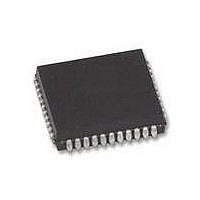
IC UART CMOS DUAL 44PLCC
Manufacturer
Exar Corporation
Type
CMOS Dual Channel UARTr
Datasheet
1.XR88C681CP40-F.pdf
(101 pages)
Specifications of XR88C681J-F
Number Of Channels
2, DUART
Package / Case
44-LCC (J-Lead)
Features
*
Fifo's
1 Byte, 3 Byte
Voltage - Supply
5V
With Parallel Port
Yes
With Cmos
Yes
Mounting Type
Surface Mount
Data Rate
1 Mbps
Supply Voltage (max)
5.25 V
Supply Voltage (min)
4.75 V
Supply Current
15 mA
Maximum Operating Temperature
+ 85 C
Minimum Operating Temperature
- 40 C
Mounting Style
SMD/SMT
Operating Supply Voltage
5 V
Propagation Delay Time Ns
400 ns
No. Of Channels
2
Supply Voltage Range
4.75V To 5.25V
Operating Temperature Range
-40°C To +85°C
Digital Ic Case Style
PLCC
No. Of Pins
44
Filter Terminals
SMD
Rohs Compliant
Yes
Lead Free Status / RoHS Status
Lead free / RoHS Compliant
Lead Free Status / RoHS Status
Lead free / RoHS Compliant, Lead free / RoHS Compliant
Other names
1016-1329
Available stocks
Company
Part Number
Manufacturer
Quantity
Price

Company:
Part Number:
XR88C681J-F
Manufacturer:
Exar Corporation
Quantity:
10 000


44 PLCC
Rev. 2.11
30
31
32
33
34
35
36
37
40 PDIP,
CDIP
27
28
29
30
31
32
33
28 PDIP
20
21
22
23
24
(RXCA_1X)
(TXCA_16)
(TXCA-1X)
FFULL_A)
(RXRDY/
Symbol
(
X1/CLK
-
RXDA
TXDA
RTSA)
OP4
OP2
OP0
NC
X2
6
Type
O
O
O
O
O
I
I
Description
Output 4 (General Purpose Output). This output pin
can also be programmed to function as the open-drain,
active-low, “Receiver Ready” or “FIFO Full” indicator
output for Channel A. (-RXRDY_A/-FFULL_A)
Output 2 (General Purpose Output). This output pin
can also be programmed to function as any of the fol-
lowing: The Channel A Transmitter 16X or 1X clock
output (TXCA_16X or TXCA_1X), or the Channel A
Receiver 1X clock output (RXCA_1X).
Output 0 (General Purpose Output). This output pin
can also be programmed to function as the active-low,
Request-to-Send output for Channel A (-RTSA).
Transmitter Serial Data Output (Channel A). The
least significant bit of the character is transmitted first.
This output is held in the marking (high) state when the
transmitter is idle, disabled, or operating in the Local
LOOPBACK mode. If an external transmitter clock is
specified, TXCA, the data is shifted out of the TSR
(Transmitter Shift Register) on the falling the edge of
the clock.
No Connect.
Receive Serial Data Input (Channel A). The least
significant bit of the character is received first. If an
external receiver clock, RXCA, is specified, the data is
sampled on the rising edge of the clock.
Crystal Output of External Clock Input. This pin is
the connection for one side of the crystal and a capaci-
tor to ground when the internal oscillator is used. If the
oscillator is not used, an external clock signal must be
supplied at this input.
In order for the XR88C681 device to function properly,
the user must supply a signal with frequencies be-
tween 2.0MHz and 4.0MHz. This requirement can be
met by either a crystal oscillator or by the external
TTL-compatible clock signal.
Crystal Input. Connection for the one side of the crys-
tal (opposite of X1/CLK). If the oscillator is used, a
capacitor must also be connected from this pin to
ground. This pin must be left open if an external clock
is supplied at X1/CLK.
Related parts for XR88C681J-F
Image
Part Number
Description
Manufacturer
Datasheet
Request
R

Part Number:
Description:
BiCMOS Fixed, Quad, Voltage Output, Single or Dual Supply 8-Bit Digital-to-Analog Converter
Manufacturer:
Exar Corporation
Datasheet:
Part Number:
Description:
Manufacturer:
Exar Corporation
Datasheet:
Part Number:
Description:
Voltage-Controlled Oscillator
Manufacturer:
Exar Corporation
Datasheet:
Part Number:
Description:
INTEGRATED LINE TRANSMITTER
Manufacturer:
Exar Corporation
Datasheet:
Part Number:
Description:
Monolithic Function Generator
Manufacturer:
Exar Corporation
Datasheet:
Part Number:
Description:
CMOS Microprocessor Compatible Double-Buffered 12-Bit Digital-to-Analog Converter
Manufacturer:
Exar Corporation
Datasheet:
Part Number:
Description:
CMOS 6 BIT HIGH SPEED ANALOG TO DIGITAL CONVERTER
Manufacturer:
Exar Corporation
Datasheet:
Part Number:
Description:
Manufacturer:
Exar Corporation
Datasheet:
Part Number:
Description:
Manufacturer:
Exar Corporation
Datasheet:
Part Number:
Description:
8-Channel, Voltage Output 10 MHz Input Bandwidth 8-Bit Multiplying DACs with Serial Digital Data Por
Manufacturer:
Exar Corporation
Datasheet:
Part Number:
Description:
15 V CMOS Multiplying10-Bit Digital-to-Analog Converter
Manufacturer:
Exar Corporation
Datasheet:
Part Number:
Description:
Monolithic Function Generator
Manufacturer:
Exar Corporation
Datasheet:
Part Number:
Description:
CMOS, 6-Bit High-Speed Analog-to-digital Converter
Manufacturer:
Exar Corporation
Datasheet: