M52277EVB Freescale Semiconductor, M52277EVB Datasheet - Page 25
M52277EVB
Manufacturer Part Number
M52277EVB
Description
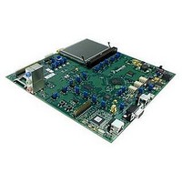
BOARD DEMO FOR MCF5227
Manufacturer
Freescale Semiconductor
Series
ColdFire®r
Type
MCUr
Specifications of M52277EVB
Contents
Board
Silicon Manufacturer
Freescale
Core Architecture
Coldfire
Core Sub-architecture
Coldfire V2
Silicon Core Number
MCF52
Silicon Family Name
MCF5227x
Peak Reflow Compatible (260 C)
Yes
Rohs Compliant
Yes
For Use With/related Products
MCF52277
Lead Free Status / RoHS Status
Lead free / RoHS Compliant


5.7.2.2
When using the SDRAM controller in DDR mode, the following timing numbers must be followed to properly latch or drive
data onto the memory bus. All timing numbers are relative to the two DQS byte lanes.
Freescale Semiconductor
Num
DD1
DD2
DD3
DD4
DD5
DD6
DD7
SD_SDR_DQS
SD_DQS[3:2]
Frequency of Operation
Clock Period
Pulse Width High
Pulse Width Low
Address, SD_CKE, SD_CAS, SD_RAS, SD_WE,
SD_CS[1:0] - Output Valid
Address, SD_CKE, SD_CAS, SD_RAS, SD_WE,
SD_CS[1:0] - Output Hold
Write Command to first DQS Latching Transition
Data and Data Mask Output Setup (DQ→DQS)
Relative to DQS (DDR Write Mode)
SD_BA[1:0]
SD_RAS,
SD_CAS,
SD_CSn,
Memories
SD_CLK
SD_CLK
SD_WE
Delayed
A[23:0],
D[31:0]
SDDM
from
DDR SDRAM AC Timing Specifications
(Measured at Output Pin)
(Measured at Input Pin)
NOTE: Data driven from memories relative
SD4
Characteristic
to delayed memory clock.
MCF5227x ColdFire
ROW
CMD
SD1
Table 15. DDR Timing Specifications
SD5
Figure 12. SDR Read Timing
®
COL
Microprocessor Data Sheet, Rev. 8
3/4 MCLK
Reference
t
Board Delay
t
t
Symbol
SDCHACV
SDCHACI
CMDVDQ
t
t
t
DQDMV
t
DDCKH
t
DDCKL
DDCK
DDSK
Board Delay
SD10
12.0
0.45
0.45
WD1
Min
2.0
1.5
60
—
—
SD2
SD6
tDQS
SD9
0.5 × SD_CLK
WD2
83.33
16.67
+ 1.0
Max
0.55
0.55
1.25
—
—
SD7
Electrical Characteristics
SD8
WD3
SD_CLK
SD_CLK
SD_CLK
SD3
Unit
MHz
ns
ns
ns
ns
WD4
Notes
1
2
3
3
4
5
6
25
Related parts for M52277EVB
Image
Part Number
Description
Manufacturer
Datasheet
Request
R

Part Number:
Description:
Manufacturer:
Freescale Semiconductor, Inc
Datasheet:
Part Number:
Description:
Manufacturer:
Freescale Semiconductor, Inc
Datasheet:
Part Number:
Description:
Manufacturer:
Freescale Semiconductor, Inc
Datasheet:
Part Number:
Description:
Manufacturer:
Freescale Semiconductor, Inc
Datasheet:
Part Number:
Description:
Manufacturer:
Freescale Semiconductor, Inc
Datasheet:
Part Number:
Description:
Manufacturer:
Freescale Semiconductor, Inc
Datasheet:
Part Number:
Description:
Manufacturer:
Freescale Semiconductor, Inc
Datasheet:
Part Number:
Description:
Manufacturer:
Freescale Semiconductor, Inc
Datasheet:
Part Number:
Description:
Manufacturer:
Freescale Semiconductor, Inc
Datasheet:
Part Number:
Description:
Manufacturer:
Freescale Semiconductor, Inc
Datasheet:
Part Number:
Description:
Manufacturer:
Freescale Semiconductor, Inc
Datasheet:
Part Number:
Description:
Manufacturer:
Freescale Semiconductor, Inc
Datasheet:
Part Number:
Description:
Manufacturer:
Freescale Semiconductor, Inc
Datasheet:
Part Number:
Description:
Manufacturer:
Freescale Semiconductor, Inc
Datasheet:
Part Number:
Description:
Manufacturer:
Freescale Semiconductor, Inc
Datasheet: