M52277EVB Freescale Semiconductor, M52277EVB Datasheet - Page 6
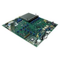
M52277EVB
Manufacturer Part Number
M52277EVB
Description
BOARD DEMO FOR MCF5227
Manufacturer
Freescale Semiconductor
Series
ColdFire®r
Type
MCUr
Specifications of M52277EVB
Contents
Board
Silicon Manufacturer
Freescale
Core Architecture
Coldfire
Core Sub-architecture
Coldfire V2
Silicon Core Number
MCF52
Silicon Family Name
MCF5227x
Peak Reflow Compatible (260 C)
Yes
Rohs Compliant
Yes
For Use With/related Products
MCF52277
Lead Free Status / RoHS Status
Lead free / RoHS Compliant


Hardware Design Considerations
3.3
To minimize noise, an external filters is required for the ADCV
between the board EV
pin as possible.
3.4
The relationship between SDV
or 3.3V) and EV
3.4.1
If EV
connected to the EV
before IV
or there will be high current in the internal ESD protection diodes. The rise times on the power supplies should be slower than
500 us to avoid turning on the internal ESD protection clamp diodes.
3.4.2
If IV
impedance state. There is no limit on how long after IV
down. IV
undesired high current in the ESD protection diodes. There are no requirements for the fall times of the power supplies.
The recommended power down sequence is as follows:
6
1.
2.
DD
DD
/PLLV
/SDV
Drop IV
Drop EV
DD
DD
ADC Power Filtering
Supply Voltage Sequencing
must powered up. IV
should not lag EV
DD
Power Up Sequence
Power Down Sequence
DD
DD
DD
are powered up with IV
are powered down first, then sense circuits in the I/O pads will cause all output drivers to be in a high
DD
are specified relative to IV
DD
/PLLV
/SDV
DD
/SDV
and the ADCV
DD
DD
DD
Board EV
supplies.
to 0 V.
DD
DD
to be in a high impedance state. There is no limit on how long after EV
MCF5227x ColdFire
DD
, SDV
and EV
should not lead the EV
DD
DD
DD
DD
DD
, or PLLV
pin. The resistor and capacitors should be placed as close to the dedicated ADCV
Figure 4. ADC V
at 0 V, then the sense circuits in the I/O pads will cause all pad output drivers
is non-critical during power-up and power-down sequences. Both SDV
DD
0 Ω
.
DD
®
DD
Microprocessor Data Sheet, Rev. 8
going low by more than 0.4 V during power down or there will be
and PLLV
DD
10 µF
, SDV
DD
GND
DD
power pin. The filter shown in
Power Filter
DD
DD
or PLLV
power down before EV
0.1 µF
DD
by more than 0.4 V during power ramp-up,
ADC V
DD
Figure 4
DD
or SDV
Pin
Freescale Semiconductor
DD
should be connected
/SDV
DD
must power
DD
powers up
DD
(2.5V
DD
Related parts for M52277EVB
Image
Part Number
Description
Manufacturer
Datasheet
Request
R

Part Number:
Description:
Manufacturer:
Freescale Semiconductor, Inc
Datasheet:
Part Number:
Description:
Manufacturer:
Freescale Semiconductor, Inc
Datasheet:
Part Number:
Description:
Manufacturer:
Freescale Semiconductor, Inc
Datasheet:
Part Number:
Description:
Manufacturer:
Freescale Semiconductor, Inc
Datasheet:
Part Number:
Description:
Manufacturer:
Freescale Semiconductor, Inc
Datasheet:
Part Number:
Description:
Manufacturer:
Freescale Semiconductor, Inc
Datasheet:
Part Number:
Description:
Manufacturer:
Freescale Semiconductor, Inc
Datasheet:
Part Number:
Description:
Manufacturer:
Freescale Semiconductor, Inc
Datasheet:
Part Number:
Description:
Manufacturer:
Freescale Semiconductor, Inc
Datasheet:
Part Number:
Description:
Manufacturer:
Freescale Semiconductor, Inc
Datasheet:
Part Number:
Description:
Manufacturer:
Freescale Semiconductor, Inc
Datasheet:
Part Number:
Description:
Manufacturer:
Freescale Semiconductor, Inc
Datasheet:
Part Number:
Description:
Manufacturer:
Freescale Semiconductor, Inc
Datasheet:
Part Number:
Description:
Manufacturer:
Freescale Semiconductor, Inc
Datasheet:
Part Number:
Description:
Manufacturer:
Freescale Semiconductor, Inc
Datasheet: