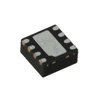
SKY65084-360LF Skyworks Solutions Inc, SKY65084-360LF Datasheet - Page 2

SKY65084-360LF
Manufacturer Part Number
SKY65084-360LF
Description
IC AMP 1.5-2.4GHZ LN 8QFN
Manufacturer
Skyworks Solutions Inc
Datasheet
1.SKY65084-360LF.pdf
(11 pages)
Specifications of SKY65084-360LF
Current - Supply
65mA
Frequency
1.5GHz ~ 2.4GHz
Gain
25dB
Noise Figure
0.7dB
P1db
16dBm
Package / Case
8-VQFN Exposed Pad
Rf Type
CDMA, GSM, WCDMA
Test Frequency
1.95GHz
Voltage - Supply
4.75 V ~ 5.25 V
Lead Free Status / RoHS Status
Lead free / RoHS Compliant
Other names
863-1269-2
Available stocks
Company
Part Number
Manufacturer
Quantity
Price
Part Number:
SKY65084-360LF
Manufacturer:
SKYWORKS/思佳讯
Quantity:
20 000
DATA SHEET • SKY65084-360LF LOW NOISE AMPLIFIER
Table 1. SKY65084-360LF Signal Descriptions
Functional Description
The SKY65084-360LF is a two stage, low noise amplifier with an
integrated interstage matching network. The device has a tested
low NF of 0.70 dB and gain of 24 dB. The device allows designers
to adjust current and gain without degrading the NF.
The external matching network largely dictates the RF
performance of the device. The matching network is required for
operation and special care should be taken when designing a
circuit board layout for the SKY65084-360LF. There are four
separate groups of external components: input, output, biasing,
and feedback. Figure 3 illustrates the circuit-on-die inside the
2 x 2 mm QFN package.
Biasing
To properly bias a depletion mode pHEMT, both the gate and
drain of the device must be biased properly. At V
V
the maximum amount of current, I
recommended to ensure proper performance.
To eliminate the need for a negative DC supply, self-biasing
should be used when a resistor is placed between one of the
2
DS
Pin #
> 2 V, the amplifier stage is in its saturated state and draws
1
2
3
4
VDD1
RFIN
BIAS1
BIAS2
Skyworks Solutions, Inc. • Phone [781] 376-3000 • Fax [781] 376-3100 • sales@skyworksinc.com • www.skyworksinc.com
Name
March 31, 2010 • Skyworks Proprietary Information • Products and Product Information are Subject to Change Without Notice • 201107E
1
RF input
Source lead for 1
Source lead for 2
st
stage DC power supply
DSS
. A V
DS
Figure 3. SKY65084-360LF On-Die Functional Diagram
of 5 V is
Description
st
nd
stage transistor
stage transistor
1
2
3
4
GS
= 0 V and
Inter-Stage
Match
Pin #
source leads and ground. A bypass capacitor should be placed in
parallel to this resistor to provide an RF ground and to ensure
performance remains unchanged at the operating frequency.
When current flows from drain to source and through the resistor,
the source voltage becomes biased above DC ground. The gate
pin of the device should be left unbiased at 0 V, which creates the
desired negative V
eliminating the need for a second DC supply. Values for resistor
components R1 and R2 can be changed to easily increase or
decrease the bias current to a desired level.
The first stage is biased at 20 percent of I
NF performance. The gain and current of the 2
can be adjusted without degrading the overall NF. More current in
the 2
Components L3 and L4 are the RF bias choke inductors (refer to
Figure 18). These are required to block RF power and pass V
the drain of each amplifier stage. Components C5, C6, C7, C9,
and C10 are RF bypass capacitors. R3 and R4 reduce the voltage
presented at the drain of each stage of the device. The resistor
values are optimized for 3
and P1dB performance.
5
6
7
8
nd
stage yields better IP3 performance.
FEEDBACK
N/C
RFOUT/VDD2
N/C
Name
S1500
8
7
6
5
GS
value. This simplifies the design by
rd
Connect to RFOUT to reduce gain of 2
stage transistor
choke inductor.
Order Output Intercept Point (OIP3)
No connection
RF output. Requires a DC bias using an RF
No connection
Description
DSS
to achieve the best
nd
stage amplifier
nd
DD
to


