SBF-5089Z Sirenza Microdevices Inc, SBF-5089Z Datasheet
SBF-5089Z
Specifications of SBF-5089Z
Available stocks


Related parts for SBF-5089Z


SBF-5089Z Summary of contents
Page 1
... InGaP/GaAs HBT MMIC Amplifier Product Description RFMD’s SBF-5089( high performance InGaP/GaAs Heterojunction Bipolar Transistor MMIC Amplifier. A Darlington configuration designed with InGaP process technology provides broadband performance up to 0.5GHz with excellent thermal performance. The heterojunction increases breakdown voltage and minimizes leak- age current between junctions ...
Page 2
... SBF-5089(Z) Absolute Maximum Ratings Parameter Device Current ( Device Voltage ( Input Power Max Operating Dissipated Power Junction Temp ( Operating Temp Range ( Storage Temp ESD Rating - Human Body Model (HBM) Moisture Sensitivity Level Operation of this device beyond any one of these limits may cause permanent dam- age ...
Page 3
... RFMD at (+1) 336-678-5570 or sales-support@rfmd.com. EDS-103413 Rev 650 750 850 Noise Figure vs Temp 5 4.5 4 3.5 3 2.5 2 1.5 +25c 1 -40c +85c 0 150 250 350 450 550 650 Frequency(MHz) SBF-5089(Z) TOIP vs Temp +25c -40c +85c 150 250 350 450 550 650 750 Frequency(MHz) 750 850 850 ...
Page 4
... SBF-5089(Z) Test Conditions: V =8V, R =33Ω BIAS S vs. Frequency 11 -10 -12 -14 -16 -18 -20 -22 -24 -26 -28 -30 50 150 250 350 450 550 Frequency (MHz) S vs. Frequency 12 -20 -20.5 -21 -21.5 -22 -22.5 -23 -23.5 -24 -24.5 -25 50 150 250 350 450 550 Frequency (MHz) 100 Note: Output Return Loss can be improved at low end of band with L1 selection. ...
Page 5
... Thorndike Road, Greensboro, NC 27409-9421 · For sales or technical support, contact RFMD at (+1) 336-678-5570 or sales-support@rfmd.com. EDS-103413 Rev E Application Circuit Schematic 1000 SBF-5089 100MHz 240MHz 500MHz 1000pF 1000pF 100pF 100pF 1.2uH 1.2uH 6.8nH 6.8nH =90mA SBF-5089( out C B 850MHz 220pF 100pF 100pF 68pF 68nH 33nH 6.8nH 6.8nH ...
Page 6
... SBF-5089(Z) Mounting Instructions 1. Note: For broadband RF unconditional stability do not put GND vias under the exposed backside GND paddle. 2. Solder the copper pad on the backside of the device package to the ground plane. 3. USe a large ground pad area with many plated through-holes as shown recommend ounce copper. Measurement for this data sheet were made on a 31mil thick FR-4 board with 1 ounce copper on both sides ...
Page 7
... Suggested Pad Layout 0.3255 [8.27] 0.0750 [1.91] (2X) 0.0640 [1.63] 0.0540 [1.37] (2X) 0.0250 [0.64] 0.0800 [2.03] 0.0420 [1.07] 0.0270 [0.69] 0.0540 [1.37] D EVICE CE NTER LINE Package Drawing Dimensions in inches (millimeters) SBF-5089(Z) (2X) (2X) 0.2560 [6.50] 0.0450 [1.14] 0.0600 [1.52] Ø0.0200 [Ø0.51] GND Via ...
Page 8
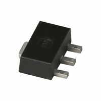
... SBF-5089(Z) Alternate marking “SBF5089” or “SBF5089Z” on line one with Trace Code on line two. Part Number SBF-5089 SBF-5089Z 7628 Thorndike Road, Greensboro, NC 27409-9421 · For sales or technical support, contact RFMD at (+1) 336-678-5570 or sales-support@rfmd.com Part Identification Lead Lead Fr ee Ordering Information Reel Size Devices/Reel 7” ...