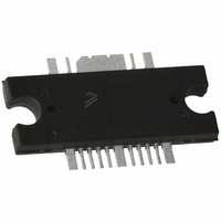
MWIC930NR1 Freescale Semiconductor, MWIC930NR1 Datasheet
MWIC930NR1
Specifications of MWIC930NR1
Available stocks


Related parts for MWIC930NR1


MWIC930NR1 Summary of contents
Page 1
... Freescale Semiconductor Technical Data Replaced by MWIC930NR1(GNR1). There are no form, fit or function changes with this part replacement. N suffix added to part number to indicate transition to lead - free terminations. RF LDMOS Wideband Integrated Power Amplifiers The MWIC930 wideband integrated circuit is designed for CDMA and GSM/GSM EDGE applications. It uses Freescale’s newest High Voltage ( Volts) LDMOS IC technology and integrates a multi - stage structure ...
Page 2
... Package Peak Temperature Unit 260 °C Min Typ Max Unit = 240 mA Avg CDMA, DQ2 out 28 31 — — % — — dBc — — % ±2.5 ±2.5 — 0.3 — dB — 0.6 — ° — 3 — ns — ±15 — ° (continued) RF Device Data Freescale Semiconductor ...
Page 3
... Input Return Loss @ out Intermodulation Distortion ( Tone, 100 kHz Tone Spacing) Intermodulation Distortion ( Tone, 100 kHz Tone Spacing) Gain Flatness MHz Bandwidth @ P Deviation from Linear Phase MHz Bandwidth @ P RF Device Data Freescale Semiconductor continued) = 25°C, unless otherwise noted Symbol P1dB G ps PAE IRL ...
Page 4
... Microstrip PCB Rogers 4350, 0.020″, ε Description Part Number ATC600S150JW ATC600S6R8CW ATC600S8R2CW ATC600S5R6CW ATC600S470JW GRM42- 2X7R105K050AL C0603C103J5R RM73B2AT102J RM73B2BT105J OUTPUT Z10 = 3.50 r Manufacturer ATC ATC ATC ATC Murata Kemet KOA Speer KOA Speer RF Device Data Freescale Semiconductor ...
Page 5
... R4 C14 V G2 Freescale has begun the transition of marking Printed Circuit Boards (PCBs) with the Freescale Semiconductor signature/logo. PCBs may have either Motorola or Freescale markings during the transition period. These changes will have no impact on form, fit or function of the current product. Figure 4. MWIC930R1(GR1) Test Circuit Component Layout ...
Page 6
... Vdc = 240 OUTPUT POWER (WATTS) out T = −30_C C 25_C 85_C Vdc (CW) out DQ1 I = 240 mA DQ2 750 800 850 900 950 f, FREQUENCY (MHz Vdc = 85_C C = 240 mA −30_C OUTPUT POWER (WATTS) out versus Output Power RF Device Data Freescale Semiconductor 35 40 1000 25_C 9 10 ...
Page 7
... P , OUTPUT POWER (WATTS) out Figure 11. Power Added Efficiency versus Output Power RF Device Data Freescale Semiconductor TYPICAL CHARACTERISTICS −30_C C 25_C 56 85_C Vdc DQ1 I = 240 mA 42 DQ2 f = 880 MHz 700 750 Figure 12. Power Added Efficiency versus T = −30_C C 25_C 85_C Vdc (CW) out DQ1 I = 240 mA ...
Page 8
... Device input impedance as measured from in RF input to ground. = Test circuit impedance as measured load from drain to ground. Output Device Matching Under Test Network load RF Device Data Freescale Semiconductor ...
Page 9
... High Q Capacitors C6, C13, C14, C15 1 μF Chip Capacitors C10, C11, C12 10 nF Chip Capacitors R1 kW, 1/8 W Chip Resistors R3 MW, 1/4 W Chip Resistors * For output matching and bypass purposes strongly recommended to use these exact capacitors. RF Device Data Freescale Semiconductor DRIVER/PRE- DRIVER PERFORMANCE ...
Page 10
... TYPICAL CHARACTERISTICS DRIVER/PRE- DRIVER PERFORMANCE ACPR System Noise Floor Vdc 105 mA 230 mA DQ1 DQ2 f = 880 MHz N−CDMA IS−95 Pilot, Sync, Paging, Traffic Codes 8 Through OUTPUT POWER (dBm) out Figure 15. Single - Carrier N - CDMA ACPR versus Output Power 30 RF Device Data Freescale Semiconductor ...
Page 11
... MHz f = 960 MHz Figure 16. Series Equivalent Input and Load Impedance — Alternate Characterization for Driver/Pre - Driver Performance RF Device Data Freescale Semiconductor Ω load Vdc 105 mA 230 mA DQ1 DQ2 out MHz Ω 740 53.944 + j6.745 2.535 + j1.662 54.452 + j7.112 760 2.602 + j1.080 780 55 ...
Page 12
... MWIC930R1 MWIC930GR1 12 NOTES RF Device Data Freescale Semiconductor ...
Page 13
... RF Device Data Freescale Semiconductor NOTES MWIC930R1 MWIC930GR1 13 ...
Page 14
... MWIC930R1 MWIC930GR1 14 PACKAGE DIMENSIONS RF Device Data Freescale Semiconductor ...
Page 15
... RF Device Data Freescale Semiconductor MWIC930R1 MWIC930GR1 15 ...
Page 16
... MWIC930R1 MWIC930GR1 16 RF Device Data Freescale Semiconductor ...
Page 17
... RF Device Data Freescale Semiconductor MWIC930R1 MWIC930GR1 17 ...
Page 18
... MWIC930R1 MWIC930GR1 18 RF Device Data Freescale Semiconductor ...
Page 19
... RF Device Data Freescale Semiconductor MWIC930R1 MWIC930GR1 19 ...
Page 20
... Freescale Semiconductor product could create a situation where personal injury or death may occur. Should Buyer ...