BGA 771L16 E6327 Infineon Technologies, BGA 771L16 E6327 Datasheet
BGA 771L16 E6327
Specifications of BGA 771L16 E6327
BGA771L16E6327XT
SP000417116


Related parts for BGA 771L16 E6327

BGA 771L16 E6327 Summary of contents
Page 1
...
Page 2
... Infineon Technologies Office. Infineon Technologies Components may only be used in life-support devices or systems with the express written approval of Infineon Technologies failure of such components can reasonably be expected to cause the failure of that life-support device or system affect the safety or effectiveness of that device or system. Life support devices or systems are intended to be implanted in the human body support and/or maintain and sustain and/or protect human life ...
Page 3
BGA771L16 Revision History: 2008-08-26, V3.0 Previous Version: 2008-07-17, V2.1 preliminary Page Subjects (major changes since last revision) 6 Updated value for thermal resistance 8 Added supply current characteristics Data Sheet BGA771L16 - Low Power Dual-Band UMTS LNA 3 V3.0, 2008-08-26 ...
Page 4
Table of Contents Table of Contents . . . . . . . . . . . . . . . . . . . . . . . . . . . . . . . . . . ...
Page 5
Description The BGA771L16 is a highly flexible, high linearity dual-band (1900/1800/2100, 800/900 MHz) low noise amplifier MMIC for worldwide use. Based on Infineon’s proprietary and cost-effective SiGe:C technology, the BGA771L16 uses an advanced biasing concept in order to achieve ...
Page 6
Electrical Characteristics 2.1 Absolute Maximum Ratings Table 1 Absolute Maximum Ratings Parameter Symbol V Supply voltage CC I Supply current CC V Pin voltage PIN V Pin voltage RF Input Pins RFIN P RF input power RFIN T Junction ...
Page 7
DC Characteristics Table 4 DC Characteristics, Parameter Symbol V Supply voltage CC I Supply current high gain CCHG mode I Supply current low gain CCLG mode I Supply current standby CCOFF mode V Logic level high HI V Logic ...
Page 8
Supply current characteristics; Supply current high / mid gain mode versus reference resistor R resistor; low gain mode supply current is independent of reference resistor). I Supply Current Midband = 2 ...
Page 9
Logic Signal Characteristics; Current consumption of logic inputs VEN1, VEN2, VGS I V Logic currents = f( ) EN1,2 EN1 2 0.5 1 1.5 V [V] EN1,2 ...
Page 10
Measured RF Characteristics Low Band 2.9.1 Measured RF Characteristics UMTS Bands Table 8 Typical Characteristics 800 MHz Band, Parameter Pass band range band V Pass band range band VI Current consumption Gain 1) Reverse Isolation Noise ...
Page 11
Measured RF Characteristics UMTS Band VIII Table 9 Typical Characteristics 900 MHz Band, Parameter Pass band range Current consumption Gain 1) Reverse Isolation Noise figure 1) Input return loss 1) Output return loss 2) Stability factor 1) Input compression ...
Page 12
Measured RF Characteristics Mid Band 2.10.1 Measured RF Characteristics UMTS Band II Table 10 Typical Characteristics 1900 MHz Band, Parameter Pass band range Current consumption Gain 1) Reverse Isolation Noise figure 1) Input return loss 1) Output return loss ...
Page 13
Measured RF Characteristics UMTS Bands III / IX Table 11 Typical Characteristics 1800 MHz Band, Parameter Pass band range band III Pass band range band IX Current consumption Gain 1) Reverse Isolation Noise figure 1) Input return loss 1) ...
Page 14
Measured RF Characteristics UMTS Band IV Table 12 Typical Characteristics 2100 MHz Band, Parameter Pass band range Current consumption Gain 1) Reverse Isolation Noise figure 1) Input return loss 1) Output return loss 2) Stability factor 1) Input compression ...
Page 15
Measured Performance Low Band (Band V) High Gain Mode vs. Frequency ° Power Gain | = ...
Page 16
Measured Performance Low Band (Band V) High Gain Mode vs. Temperature NF f Noise Figure = 1.6 1.5 1.4 1.3 1.2 1.1 1 0.9 0.8 0.86 0.87 0.88 Frequency [GHz] 2.12 Measured Performance Low Band (Band V) ...
Page 17
NF T Noise Figure = 1.8 1.6 1.4 1.2 1 0.8 0.6 −40 − [°C] A 2.13 Measured Performance Low Band (Band V) Low Gain Mode vs. Frequency ...
Page 18
Matching | | = −5 −10 −15 −20 −25 −30 0.86 0.87 0.88 Frequency [GHz Noise Figure = ...
Page 19
Measured Performance Low Band (Band V) Low Gain Mode vs. Temperature 2.14 Measured Performance Low Band (Band V) Low Gain Mode vs. Temperature 2 EN1 |S T ...
Page 20
Measured Performance Mid Band (Band II) High Gain Mode vs. Frequency ° Power Gain | = ...
Page 21
Measured Performance Mid Band (Band II) High Gain Mode vs. Temperature NF f Noise Figure = 1.6 1.5 1.4 1.3 1.2 1.1 1 0.9 0.8 1.93 1.94 1.95 1.96 Frequency [GHz] 2.16 Measured Performance Mid Band (Band ...
Page 22
NF T Noise Figure = 1.8 1.6 1.4 1.2 1 0.8 0.6 −40 − [°C] A 2.17 Measured Performance Mid Band (Band II) Low Gain Mode vs. Frequency ...
Page 23
Matching | | = −5 −10 −15 −20 −25 −30 1.93 1.94 1.95 1.96 Frequency [GHz Noise Figure = ...
Page 24
Measured Performance Mid Band (Band II) Low Gain Mode vs. Temperature 2.18 Measured Performance Mid Band (Band II) Low Gain Mode vs. Temperature 2 2 EN1 |S T ...
Page 25
Application Circuit and Block Diagram 3.1 UMTS bands II and V Application Circuit Schematic RFIN L1 Band II L1 3.3nH RFIN Band V Figure 2 Application circuit with chip outline (top view) ...
Page 26
UMTS bands III and VIII Application Circuit Schematic C1 22pF RFIN L1 Band III L1 4 .3nH C2 22pF L1 3.3 pF RFIN Band VIII Figure 3 Application circuit with chip outline (top view) Note: Package paddle (Pin 0) ...
Page 27
UMTS bands IV and VIII Application Circuit Schematic C1 22pF RFIN L1 Band 22pF L1 3.3 pF RFIN Band VIII Figure 4 Application circuit with chip outline (top view) Note: Package paddle (Pin 0) ...
Page 28
Pin Definition Table 16 Pin Definition and Function Pin Number Symbol 0 GND 1 n/c 2 VGS 3 VCC 4 n/c 5 n/c 6 RFINM 7 n/c 8 RFGNDM 9 n/c 10 RFINL 11 VEN2 12 VEN1 13 RREF ...
Page 29
Application Board Figure 5 Application board layout on 3-layer FR4. Top layer thickness: 0.2 mm, bottom layer thickness: 0.8 mm metallization, gold plated. Board size Figure 6 Cross-section view of application board ...
Page 30
Figure 7 Detail of application board layout Note: In order to achieve the same performance as given in this datasheet please follow the suggested PCB-layout as closely as possible. The position of the GND vias is critical for RF performance. ...
Page 31
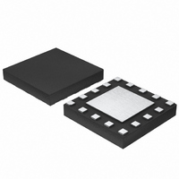
Physical Characteristics 4.1 Package Footprint 0.225 0.3 0.2 0.3 0.3 Copper 0.35 0.225 0.3 0.2 0.3 0.3 Copper Figure 8 Recommended footprint and stencil layout for the TSLP-16-1 package Data Sheet BGA771L16 - ...
Page 32
Package Dimensions Top view Pin 1 marking 1) Dimension applies to plated terminals Figure 9 Package outline (top, side and bottom view) Data Sheet BGA771L16 - Low Power Dual-Band UMTS LNA Bottom view +0.01 0.39 -0.03 0.05 MAX. 9 ...
Page 33
... Published by Infineon Technologies AG ...