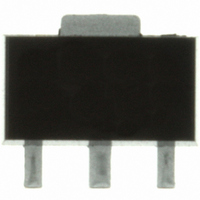
MMG3002NT1 Freescale Semiconductor, MMG3002NT1 Datasheet

MMG3002NT1
Specifications of MMG3002NT1
MMG3002NT1TR
Available stocks
Related parts for MMG3002NT1
MMG3002NT1 Summary of contents
Page 1
... Heterojunction Bipolar Transistor Technology (InGaP HBT) Broadband High Linearity Amplifier The MMG3002NT1 is a General Purpose Amplifier that is internally input and output matched designed for a broad range of Class A, small - signal, high linearity, general purpose applications suitable for applications with frequencies from 40 to 3600 MHz such as Cellular, PCS, BWA, WLL, PHS, CATV, VHF, UHF, UMTS and general small - signal RF ...
Page 2
... Output Return Loss (S22) Power Output @ 1dB Compression Third Order Output Intercept Point Noise Figure (1) Supply Current (1) Supply Voltage 1. For reliable operation, the junction temperature should not exceed 150°C. MMG3002NT1 2 = 5.2 Vdc, 900 MHz 25°C, 50 ohm system, in Freescale Application Circuit Symbol G p ...
Page 3
... Machine Model (per EIA/JESD 22 - A115) Charge Device Model (per JESD 22 - C101) Table 7. Moisture Sensitivity Level Test Methodology Per JESD 22 - A113, IPC/JEDEC J - STD - 020 RF Device Data Freescale Semiconductor Figure 1. Functional Diagram Class 1B (Minimum) A (Minimum) IV (Minimum) Rating Package Peak Temperature 1 260 Unit °C MMG3002NT1 3 ...
Page 4
... Figure 4. Small - Signal Gain versus Output Power 160 140 120 100 4.6 4.7 4.8 4 COLLECTOR VOLTAGE (V) CC Figure 6. Collector Current versus Collector Voltage MMG3002NT1 4 50 OHM TYPICAL CHARACTERISTICS 0 −10 −20 − 5.2 Vdc CC − Figure 3. Input/Output Return Loss versus ...
Page 5
... T, TEMPERATURE (_C) versus Case Temperature 125 130 135 140 145 T , JUNCTION TEMPERATURE (° 5.2 Vdc 110 5.2 Vdc 110 mA 2140 MHz CC CC Single−Carrier W−CDMA, 3.84 MHz Channel Bandwidth Input Signal PAR = 8 0.01% Probability (CCDF OUTPUT POWER (dBm) out MMG3002NT1 80 100 150 19 5 ...
Page 6
... Chip Capacitor C4 1 μF Chip Capacitor L1 470 nH Chip Inductor R1 7.5 W Chip Resistor Table 9. Supply Voltage versus R1 Values Supply Voltage 6 R1 Value 7.3 Note: To provide V = 5.2 Vdc and I CC MMG3002NT1 6 V SUPPLY R1 L1 DUT 0.403″ x 0.058″ Microstrip PCB Getek Grade ML200C, 0.031″ ...
Page 7
... Getek Grade ML200C, 0.031″, ε Figure 17. 50 Ohm Test Circuit Schematic 5.2 Vdc 110 mA CC 2800 3200 3600 Figure 19. 50 Ohm Test Circuit Component Layout Description C0603C151J5RAC C0603C104J5RAC C0603C105J5RAC HK160856NJ - T RK73B2ATTE7R5J OUTPUT 4 MMG30XX Rev 2 Part Number Manufacturer Kemet Kemet Kemet Taiyo Yuden KOA Speer MMG3002NT1 7 ...
Page 8
... Chip Capacitors C3 0.1 μF Chip Capacitor C4 1 μF Chip Capacitor (1) C5 0.1 pF Chip Capacitor Chip Inductor R1 7.5 W Chip Resistor 1. Tuning capacitor: Capacitor value and location on the transmission line are varied for different frequencies. MMG3002NT1 8 V SUPPLY R1 L1 DUT 0.085″ x 0.058″ Microstrip Z5 0.404″ ...
Page 9
... MMG3002NT1 9 ...
Page 10
... MMG3002NT1 10 50 OHM TYPICAL CHARACTERISTICS (V = 5.2 Vdc 110 mA 25°C, 50 Ohm System) (continued ∠ φ 6.29055 67.098 0.07295 6.20851 65 ...
Page 11
... POSSIBLE SHOULD BE PLACED ON THE LANDING PATTERN VIAS CANNOT BE PLACED ON THE LANDING PATTERN, THEN AS MANY VIAS AS POSSIBLE SHOULD BE PLACED AS CLOSE TO THE LANDING PATTERN AS POSSIBLE FOR OPTIMAL THERMAL AND RF PERFORMANCE. 4. RECOMMENDED VIA PATTERN SHOWN HAS 0.381 x 0.762 MM PITCH. 7.62 0.305 diameter 2.49 2.54 MMG3002NT1 11 ...
Page 12
... MMG3002NT1 12 PACKAGE DIMENSIONS RF Device Data Freescale Semiconductor ...
Page 13
... RF Device Data Freescale Semiconductor MMG3002NT1 13 ...
Page 14
... MMG3002NT1 14 RF Device Data Freescale Semiconductor ...
Page 15
... Corrected Fig. 13, Single - Carrier W - CDMA Adjacent Channel Power Ratio versus Output Power y - axis (ACPR) unit of measure to dBc • Corrected S - Parameter table frequency column label to read “MHz” versus “GHz” and corrected frequency values from GHz to MHz Device Data Freescale Semiconductor PRODUCT DOCUMENTATION REVISION HISTORY Description MMG3002NT1 15 ...
Page 16
... Denver, Colorado 80217 1 - 800 - 441 - 2447 or 303 - 675 - 2140 Fax: 303 - 675 - 2150 LDCForFreescaleSemiconductor@hibbertgroup.com MMG3002NT1 Document Number: MMG3002NT1 Rev. 9, 3/2008 16 Information in this document is provided solely to enable system and software implementers to use Freescale Semiconductor products. There are no express or implied copyright licenses granted hereunder to design or fabricate any integrated circuits or integrated circuits based on the information in this document ...


