MWE6IC9100NR1 Freescale Semiconductor, MWE6IC9100NR1 Datasheet
MWE6IC9100NR1
Specifications of MWE6IC9100NR1
Available stocks


Related parts for MWE6IC9100NR1

MWE6IC9100NR1 Summary of contents
Page 1
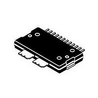
... I = 950 mA, DQ1 DQ2 = 28 Volts 230 mA DQ1 DQ2 RF /V out DS2 (1) MWE6IC9100NR1 MWE6IC9100GNR1 MWE6IC9100NBR1 Document Number: MWE6IC9100N Rev. 3, 12/2008 MWE6IC9100NR1 MWE6IC9100GNR1 MWE6IC9100NBR1 960 MHz, 100 GSM/GSM EDGE RF LDMOS WIDEBAND INTEGRATED POWER AMPLIFIERS CASE 1618 - 270 PLASTIC MWE6IC9100NR1 CASE 1621 - 270 GULL ...
Page 2
... Continuous use at maximum temperature will affect MTTF. 2. MTTF calculator available at http://www.freescale.com/rf. Select Software & Tools/Development Tools/Calculators to access MTTF calculators by product. 3. Refer to AN1955, Thermal Measurement Methodology of RF Power Amplifiers http://www.freescale.com/rf. Select Documentation/Application Notes - AN1955. MWE6IC9100NR1 MWE6IC9100GNR1 MWE6IC9100NBR1 2 Stage 1, 26 Vdc 120 mA DQ1 ...
Page 3
... GSS V GS(th) V GS(Q) V GG(Q) V DS(on Vdc 100 W CW out G ps IRL PAE P1dB G ps PAE EVM SR1 SR2 MWE6IC9100NR1 MWE6IC9100GNR1 MWE6IC9100NBR1 Min Typ Max Unit — — 10 μAdc — — 1 μAdc — — 10 μAdc 1.5 2 3.5 Vdc — 2.7 — Vdc 6 8 ...
Page 4
... Microstrip Z7 0.039″ x 0.607″ Microstrip Z8 0.555″ x 1.102″ Microstrip Z9 0.343″ x 0.083″ Microstrip Figure 3. MWE6IC9100NR1(GNR1)(NBR1) Test Circuit Schematic Table 6. MWE6IC9100NR1(GNR1)(NBR1) Test Circuit Component Designations and Values Part C1 Chip Capacitors C3, C4, C5 3.9 pF Chip Capacitors C6 0.5 pF Chip Capacitor ...
Page 5
... MWE6IC9100N V DD1 Rev. 4 C17 C22 C13 V GG1 R1 C15 R2 C16 V GG2 C18 Figure 4. MWE6IC9100NR1(GNR1)(NBR1) Test Circuit Component Layout RF Device Data Freescale Semiconductor C11 C1 C2 C14 C12 C19 MWE6IC9100NR1 MWE6IC9100GNR1 MWE6IC9100NBR1 DD2 C20 C23 C21 C24 C10 C9 5 ...
Page 6
... DQ2 590 mA DQ2 470 mA DQ2 OUTPUT POWER (WATTS) CW out Figure 7. Power Gain versus Output Power @ I = 120 mA DQ1 MWE6IC9100NR1 MWE6IC9100GNR1 MWE6IC9100NBR1 6 TYPICAL CHARACTERISTICS G ps PAE Vdc 100 out I = 120 mA 950 mA DQ1 DQ2 IRL 860 880 900 920 940 f, FREQUENCY (MHz) ...
Page 7
... Figure 14. Power Gain versus Output Power MWE6IC9100NR1 MWE6IC9100GNR1 MWE6IC9100NBR1 = 26 Vdc 100 W (PEP 150 mA DD out DQ1 = 1 A, Two−Tone Measurements 3rd Order 5th Order 7th Order 1 10 TWO−TONE SPACING (MHz) Figure 10. Intermodulation Distortion Products versus Tone Spacing T = − ...
Page 8
... C −80 85_C 25_C −85 − OUTPUT POWER (WATTS) out Figure 19. Spectral Regrowth at 600 kHz versus Output Power @ 945 MHz MWE6IC9100NR1 MWE6IC9100GNR1 MWE6IC9100NBR1 8 TYPICAL CHARACTERISTICS − 400 kHz −55 −60 − Avg. −70 − 600 kHz −80 −85 960 980 860 Figure 16. Spectral Regrowth at 400 kHz and − ...
Page 9
... T = −30_C OUTPUT POWER (WATTS) AVG. out versus Output Power @ 880 MHz −5 34 −10 32 −15 30 −20 28 −25 26 1200 1400 1600 820 Figure 24. Power Gain versus Frequency MWE6IC9100NR1 MWE6IC9100GNR1 MWE6IC9100NBR1 85_C 20 −30_C 10 EVM 0 100 85_C 20 10 EVM 0 100 T = −30_C C 25_C 85_C Vdc, P ...
Page 10
... Figure 25. MTTF versus Junction Temperature −10 −20 −30 −40 −50 −60 −70 −80 −90 −100 −110 MWE6IC9100NR1 MWE6IC9100GNR1 MWE6IC9100NBR1 10 TYPICAL CHARACTERISTICS 1st Stage 110 130 150 170 190 210 T , JUNCTION TEMPERATURE (°C) J This above graph displays calculated MTTF in hours when the device ...
Page 11
... Z = Test circuit impedance as measured from source gate to ground Test circuit impedance as measured load from drain to ground. Device Input Matching Under Test Network Z Z source load MWE6IC9100NR1 MWE6IC9100GNR1 MWE6IC9100NBR1 f = 980 MHz = 100 W CW out Z load W Output Matching Network 11 ...
Page 12
... MWE6IC9100NR1 MWE6IC9100GNR1 MWE6IC9100NBR1 ohm system 120 mA DQ1 ∠ φ 5. 0.0007 6. 0.0007 7.18 - 107 0.0007 7.88 - 117 0.0007 8.56 - 128 0 ...
Page 13
... RF Device Data Freescale Semiconductor PACKAGE DIMENSIONS MWE6IC9100NR1 MWE6IC9100GNR1 MWE6IC9100NBR1 13 ...
Page 14
... MWE6IC9100NR1 MWE6IC9100GNR1 MWE6IC9100NBR1 14 RF Device Data Freescale Semiconductor ...
Page 15
... RF Device Data Freescale Semiconductor MWE6IC9100NR1 MWE6IC9100GNR1 MWE6IC9100NBR1 15 ...
Page 16
... MWE6IC9100NR1 MWE6IC9100GNR1 MWE6IC9100NBR1 16 RF Device Data Freescale Semiconductor ...
Page 17
... RF Device Data Freescale Semiconductor MWE6IC9100NR1 MWE6IC9100GNR1 MWE6IC9100NBR1 17 ...
Page 18
... MWE6IC9100NR1 MWE6IC9100GNR1 MWE6IC9100NBR1 18 RF Device Data Freescale Semiconductor ...
Page 19
... RF Device Data Freescale Semiconductor MWE6IC9100NR1 MWE6IC9100GNR1 MWE6IC9100NBR1 19 ...
Page 20
... MWE6IC9100NR1 MWE6IC9100GNR1 MWE6IC9100NBR1 20 RF Device Data Freescale Semiconductor ...
Page 21
... RF Device Data Freescale Semiconductor MWE6IC9100NR1 MWE6IC9100GNR1 MWE6IC9100NBR1 21 ...
Page 22
... Replaced Case Outline 1621 - 01 with 1621 - 02, Issue 21. Added pin numbers 1, 12, 13, and 14 and Pin 1 Index designation to Sheet 1. Corrected dimensions e and e1 on Sheets 1 and 3. Removed Pin 5 designation from Sheet 2. • Added Product Documentation and Revision History MWE6IC9100NR1 MWE6IC9100GNR1 MWE6IC9100NBR1 22 PRODUCT DOCUMENTATION REVISION HISTORY Description value, p ...
Page 23
... Semiconductor was negligent regarding the design or manufacture of the part. Freescalet and the Freescale logo are trademarks of Freescale Semiconductor, Inc. All other product or service names are the property of their respective owners. © Freescale Semiconductor, Inc. 2007-2008. All rights reserved. MWE6IC9100NR1 MWE6IC9100GNR1 MWE6IC9100NBR1 23 ...