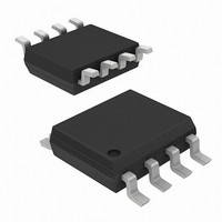
AD8361ARM Analog Devices Inc, AD8361ARM Datasheet - Page 18

AD8361ARM
Manufacturer Part Number
AD8361ARM
Description
IC PWR DETECTOR 2.5GHZ 8-MSOP
Manufacturer
Analog Devices Inc
Datasheet
1.AD8361-EVAL.pdf
(24 pages)
Specifications of AD8361ARM
Rf Type
Cellular, CDMA, W-CDMA
Rohs Status
RoHS non-compliant
Frequency
100MHz ~ 2.5GHz
Input Range
0 ~ 700mV
Accuracy
±0.25dB
Voltage - Supply
2.7 V ~ 5.5 V
Current - Supply
1.1mA
Package / Case
8-TSSOP, 8-MSOP (0.118", 3.00mm Width)
Frequency Range
100MHz To 2.5GHz
Supply Current
1.1mA
Supply Voltage Range
2.7V To 5.5V
Rf Ic Case Style
MSOP
No. Of Pins
8
Operating Temperature Range
-40°C To +85°C
Pin Count
8
Screening Level
Industrial
Package Type
MSOP
Lead Free Status / Rohs Status
Not Compliant
Available stocks
Company
Part Number
Manufacturer
Quantity
Price
Company:
Part Number:
AD8361ARM
Manufacturer:
AD
Quantity:
4 130
Part Number:
AD8361ARM
Manufacturer:
ADI/亚德诺
Quantity:
20 000
Company:
Part Number:
AD8361ARM-REEL7
Manufacturer:
AD
Quantity:
5 321
Company:
Part Number:
AD8361ARMZ
Manufacturer:
ADI
Quantity:
3 000
Company:
Part Number:
AD8361ARMZ
Manufacturer:
SOP8
Quantity:
4 800
Part Number:
AD8361ARMZ
Manufacturer:
ADI/亚德诺
Quantity:
20 000
Part Number:
AD8361ARMZ-REEL
Manufacturer:
ADI/亚德诺
Quantity:
20 000
Part Number:
AD8361ARMZ-REEL7
Manufacturer:
ADI/亚德诺
Quantity:
20 000
Part Number:
AD8361ARMZ-RL7
Manufacturer:
ADI/亚德诺
Quantity:
20 000
AD8361
–0.5
–1.0
–1.5
–2.0
–2.5
–0.5
–1.0
–1.5
–2.0
–2.5
–0.5
–1.0
–1.5
–2.0
–2.5
2.5
2.0
1.5
1.0
0.5
2.5
2.0
1.5
1.0
0.5
2.5
2.0
1.5
1.0
0.5
0
0
0
–25
–25
–25
Figure 55. Transfer Function and Error Plots Measured at
Figure 56. Transfer Function and Error Plots Measured at
Figure 57. Transfer Function and Error Plots Measured at
–20
–20
–20
–30°C
2.5 GHz for a 64 QAM Modulated Signal
–30°C
2.7 GHz for a 64 QAM Modulated Signal
3.0 GHz for a 64 QAM Modulated Signal
–30°C
–15
–15
–15
–10
–10
PIN (dBm)
PIN (dBm)
–10
PIN (dBm)
+25°C
+25 °C
+25°C
–5
–5
–5
+80°C
+80°C
+80°C
0
0
0
5
5
5
10
10
10
10
0.1
10
0.1
1
10
0.1
1
1
Rev. C | Page 18 of 24
The transfer functions and error for a CW input and a 64 QAM
input waveform is shown in Figure 58. The error curve is
generated from a linear reference based on the CW data. The
increased crest factor of the 64 QAM modulation results in a
decrease in output from the AD8361. This decrease in output is
a result of the limited bandwidth and compression of the
internal gain stages. This inaccuracy should be accounted for in
systems where varying crest factor signals need to be measured.
The conversion gain is defined as the slope of the output voltage
versus the input rms voltage. An ideal best fit curve can be
found for the measured transfer function at a given supply
voltage and temperature. The slope of the ideal curve is
identified as the conversion gain for a particular device. The
conversion gain relates the measurement sensitivity of the
AD8361 to the rms input voltage of the RF waveform. The
conversion gain was measured for a number of devices over a
temperature range of −30°C to +80°C. The conversion gain for a
typical device is shown in Figure 59. Although the conversion
gain tends to decrease with increasing frequency, the AD8361
provides measurement capability at frequencies greater than
Figure 58. Error from CW Linear Reference vs. Input Drive Level for CW
–0.5
–1.0
–1.5
–2.0
–2.5
2.5
2.0
1.5
1.0
0.5
0
–25
8.0
7.5
7.0
6.5
6.0
5.5
5.0
100
Typical Device, Supply 3 V, Ground Reference Mode
Figure 59. Conversion Gain vs. Frequency for a
–20
and 64 QAM Modulated Signals at 3.0 GHz
200
400
–15
800
FREQUENCY (MHz)
–10
PIN (dBm)
1200 1600 2200 2500 2700 3000
CW
–5
64 QAM
0
5
10
10
1
0.1


