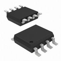
AD8361ARM Analog Devices Inc, AD8361ARM Datasheet - Page 19

AD8361ARM
Manufacturer Part Number
AD8361ARM
Description
IC PWR DETECTOR 2.5GHZ 8-MSOP
Manufacturer
Analog Devices Inc
Datasheet
1.AD8361-EVAL.pdf
(24 pages)
Specifications of AD8361ARM
Rf Type
Cellular, CDMA, W-CDMA
Rohs Status
RoHS non-compliant
Frequency
100MHz ~ 2.5GHz
Input Range
0 ~ 700mV
Accuracy
±0.25dB
Voltage - Supply
2.7 V ~ 5.5 V
Current - Supply
1.1mA
Package / Case
8-TSSOP, 8-MSOP (0.118", 3.00mm Width)
Frequency Range
100MHz To 2.5GHz
Supply Current
1.1mA
Supply Voltage Range
2.7V To 5.5V
Rf Ic Case Style
MSOP
No. Of Pins
8
Operating Temperature Range
-40°C To +85°C
Pin Count
8
Screening Level
Industrial
Package Type
MSOP
Lead Free Status / Rohs Status
Not Compliant
Available stocks
Company
Part Number
Manufacturer
Quantity
Price
Company:
Part Number:
AD8361ARM
Manufacturer:
AD
Quantity:
4 130
Part Number:
AD8361ARM
Manufacturer:
ADI/亚德诺
Quantity:
20 000
Company:
Part Number:
AD8361ARM-REEL7
Manufacturer:
AD
Quantity:
5 321
Company:
Part Number:
AD8361ARMZ
Manufacturer:
ADI
Quantity:
3 000
Company:
Part Number:
AD8361ARMZ
Manufacturer:
SOP8
Quantity:
4 800
Part Number:
AD8361ARMZ
Manufacturer:
ADI/亚德诺
Quantity:
20 000
Part Number:
AD8361ARMZ-REEL
Manufacturer:
ADI/亚德诺
Quantity:
20 000
Part Number:
AD8361ARMZ-REEL7
Manufacturer:
ADI/亚德诺
Quantity:
20 000
Part Number:
AD8361ARMZ-RL7
Manufacturer:
ADI/亚德诺
Quantity:
20 000
2.5 GHz. However, it is necessary to calibrate for a given
application to accommodate for the change in conversion gain
at higher frequencies.
Dynamic Range Extension for the AD8361
The accurate measurement range of the AD8361 is limited by
internal dc offsets for small input signals and by square law
conformance errors for large signals. The measurement range
may be extended by using two devices operating at different
signal levels and then choosing only the output of the device
that provides accurate results at the prevailing input level.
Figure 60 depicts an implementation of this idea. In this circuit,
the selection of the output is made gradually over an input level
range of about 3 dB in order to minimize the impact of
imperfect matching of the transfer functions of the two
AD8361s. Such a mismatch typically arises because of the
variation of the gain of the RF preamplifier U1 and both the
gain and slope variations of the AD8361s with temperature.
INPUT
RF
SPLITTER
6dB
6dB
PAD
12V
ERA-3
20dB
U1
270Ω
RFC
68Ω
68Ω
10kΩ
R2
0.01µF
0.01µF
100pF
100pF
5V
5V
5V
1
2
3
4
1
2
3
4
Q2
2N3906
Figure 60. Range Extender Application
1kΩ
AD8361
AD8361
12V
U2
U4
2N3906
20kΩ
Rev. C | Page 19 of 24
1kΩ
Q1
8
7
6
5
8
7
6
5
0.1µF
0.1µF
5V
5V
One of the AD8361s (U2) has a net gain of about 14 dB
preceding it and therefore operates most accurately at low input
signal levels. This is referred to as the weak signal path. U4, on
the other hand, does not have the added gain and provides
accurate response at high levels. The output of U2 is attenuated
by R1 in order to cancel the effect of U2’s preceding gain so that
the slope of the transfer function (as seen at the slider of R1) is
the same as that of U4 by itself.
The circuit comprising U3, U5, and U6 is a crossfader, in which
the relative gains of the two inputs are determined by the output
currents of a fuzzy comparator made from Q1 and Q2.
Assuming that the slider of R2 is at 2.5 V dc, the fuzzy
comparator commands full weighting of the weak signal path
when the output of U2 is below about 2.0 V dc, and full
weighting of the strong signal path when the output of U3
exceeds about 3.0 V dc. U3 and U5 are OTAs (operational
transconductance amplifiers).
–5V
12kΩ
16kΩ
20kΩ
20kΩ
5kΩ
R1
10kΩ
R3
1MΩ
2
2
3
3
+5V
CA3080
CA3080
+12V
+12V
–5V
–5V
U3
U5
5
5
6
6
100Ω
8.2nF
2
3
AD820
5V
7
4
U6
6
AD8361
V
OUT


