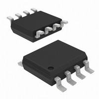
AD8361ARM Analog Devices Inc, AD8361ARM Datasheet - Page 20

AD8361ARM
Manufacturer Part Number
AD8361ARM
Description
IC PWR DETECTOR 2.5GHZ 8-MSOP
Manufacturer
Analog Devices Inc
Datasheet
1.AD8361-EVAL.pdf
(24 pages)
Specifications of AD8361ARM
Rf Type
Cellular, CDMA, W-CDMA
Rohs Status
RoHS non-compliant
Frequency
100MHz ~ 2.5GHz
Input Range
0 ~ 700mV
Accuracy
±0.25dB
Voltage - Supply
2.7 V ~ 5.5 V
Current - Supply
1.1mA
Package / Case
8-TSSOP, 8-MSOP (0.118", 3.00mm Width)
Frequency Range
100MHz To 2.5GHz
Supply Current
1.1mA
Supply Voltage Range
2.7V To 5.5V
Rf Ic Case Style
MSOP
No. Of Pins
8
Operating Temperature Range
-40°C To +85°C
Pin Count
8
Screening Level
Industrial
Package Type
MSOP
Lead Free Status / Rohs Status
Not Compliant
Available stocks
Company
Part Number
Manufacturer
Quantity
Price
Company:
Part Number:
AD8361ARM
Manufacturer:
AD
Quantity:
4 130
Part Number:
AD8361ARM
Manufacturer:
ADI/亚德诺
Quantity:
20 000
Company:
Part Number:
AD8361ARM-REEL7
Manufacturer:
AD
Quantity:
5 321
Company:
Part Number:
AD8361ARMZ
Manufacturer:
ADI
Quantity:
3 000
Company:
Part Number:
AD8361ARMZ
Manufacturer:
SOP8
Quantity:
4 800
Part Number:
AD8361ARMZ
Manufacturer:
ADI/亚德诺
Quantity:
20 000
Part Number:
AD8361ARMZ-REEL
Manufacturer:
ADI/亚德诺
Quantity:
20 000
Part Number:
AD8361ARMZ-REEL7
Manufacturer:
ADI/亚德诺
Quantity:
20 000
Part Number:
AD8361ARMZ-RL7
Manufacturer:
ADI/亚德诺
Quantity:
20 000
AD8361
U6 provides feedback to linearize the inherent tanh transfer
function of the OTAs. When one OTA or the other is fully
selected, the feedback is very effective. The active OTA has zero
differential input; the inactive one has a potentially large
differential input, but this does not matter because the inactive
OTA is not contributing to the output. However, when both
OTAs are active to some extent, and the two signal inputs to the
crossfader are different, it is impossible to have zero differential
inputs on the OTAs. In this event, the crossfader admittedly
generates distortion because of the nonlinear transfer function
of the OTAs. Fortunately, in this application, the distortion is
not very objectionable for two reasons:
1.
2.
This circuit has three trimmable potentiometers. The suggested
setup procedure is as follows:
1.
2.
3.
4.
The mismatch in input levels to the crossfader is never
large enough to evoke very much distortion because the
AD8361s are reasonably well-behaved.
The effect of the distortion in this case is merely to distort
the otherwise nearly linear slope of the transition between
the crossfader’s two inputs.
Preset R3 at midrange.
Set R2 so that its slider’s voltage is at the middle of the
desired transition zone (about 2.5 V dc is recommended).
Set R1 so that the transfer function’s slopes are equal on
both sides of the transition zone. This is perhaps best
accomplished by making a plot of the overall transfer
function (using linear voltage scales for both axes) to assess
the match in slope between one side of the transition
region and the other (see Figure 61). Note: it may be
helpful to adjust R3 to remove any large misalignment in
the transfer function in order to correctly perceive slope
differences.
Finally (re)adjust R3 as required to remove any remaining
misalignment in the transfer function (see Figure 62).
V
OUT
SLOPES INDICATE
MALADJUSTMENT
Figure 61. Slope Adjustment
m
1
DIFFERING
m
OF R1
1
≠ m
TRANSITION
2
RF INPUT LEVEL – V rms
REGION
m
2
Rev. C | Page 20 of 24
In principle, this method could be extended to three or more
AD8361s in pursuit of even more measurement range. However,
it is very important to pay close attention to the matter of not
excessively overdriving the AD8361s in the weaker signal paths
under strong signal conditions.
Figure 63 shows the extended range transfer function at multiple
temperatures. The discontinuity at approximately 0.2 V rms arises
as a result of component temperature dependencies. Figure 64
shows the error in dB of the range extender circuit at ambient
temperature. For a 1 dB error margin, the range extender circuit
offers 38 dB of measurement range.
3.0
2.5
2.0
1.5
1.0
0.5
–1
–2
–3
–4
–5
0
5
4
3
2
1
0
–32
0
Figure 63. Output vs. Drive Level over Temperature for
Figure 64. Error from Linear Reference at 25°C for a
V
OUT
–27
0.2
a 1 GHz 64 QAM Modulated Signal
1 GHz 64 QAM Modulated Signal
–22
Figure 62. Intercept Adjustment
MISALIGNMENT INDICATES
MALADJUSTMENT OF R3
–17
DRIVE LEVEL (V rms)
DRIVE LEVEL (dBm)
0.4
TRANSITION
–12
RF INPUT LEVEL – V rms
REGION
+80°C
–7
0.6
REF LINE
–2
–30°C
3
0.8
8
13
1.0


