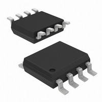
AD8361ARM Analog Devices Inc, AD8361ARM Datasheet - Page 23

AD8361ARM
Manufacturer Part Number
AD8361ARM
Description
IC PWR DETECTOR 2.5GHZ 8-MSOP
Manufacturer
Analog Devices Inc
Datasheet
1.AD8361-EVAL.pdf
(24 pages)
Specifications of AD8361ARM
Rf Type
Cellular, CDMA, W-CDMA
Rohs Status
RoHS non-compliant
Frequency
100MHz ~ 2.5GHz
Input Range
0 ~ 700mV
Accuracy
±0.25dB
Voltage - Supply
2.7 V ~ 5.5 V
Current - Supply
1.1mA
Package / Case
8-TSSOP, 8-MSOP (0.118", 3.00mm Width)
Frequency Range
100MHz To 2.5GHz
Supply Current
1.1mA
Supply Voltage Range
2.7V To 5.5V
Rf Ic Case Style
MSOP
No. Of Pins
8
Operating Temperature Range
-40°C To +85°C
Pin Count
8
Screening Level
Industrial
Package Type
MSOP
Lead Free Status / Rohs Status
Not Compliant
Available stocks
Company
Part Number
Manufacturer
Quantity
Price
Company:
Part Number:
AD8361ARM
Manufacturer:
AD
Quantity:
4 130
Part Number:
AD8361ARM
Manufacturer:
ADI/亚德诺
Quantity:
20 000
Company:
Part Number:
AD8361ARM-REEL7
Manufacturer:
AD
Quantity:
5 321
Company:
Part Number:
AD8361ARMZ
Manufacturer:
ADI
Quantity:
3 000
Company:
Part Number:
AD8361ARMZ
Manufacturer:
SOP8
Quantity:
4 800
Part Number:
AD8361ARMZ
Manufacturer:
ADI/亚德诺
Quantity:
20 000
Part Number:
AD8361ARMZ-REEL
Manufacturer:
ADI/亚德诺
Quantity:
20 000
Part Number:
AD8361ARMZ-REEL7
Manufacturer:
ADI/亚德诺
Quantity:
20 000
Part Number:
AD8361ARMZ-RL7
Manufacturer:
ADI/亚德诺
Quantity:
20 000
Problems caused by impedance mismatch may arise using the
evaluation board to examine the AD8361 performance. One
way to reduce these problems is to put a coaxial 3 dB attenuator
on the RFIN SMA connector. Mismatches at the source, cable,
and cable interconnection, as well as those occurring on the
evaluation board, can cause these problems.
A simple (and common) example of such a problem is triple
travel due to mismatch at both the source and the evaluation
board. Here the signal from the source reaches the evaluation
board and mismatch causes a reflection. When that reflection
reaches the source mismatch, it causes a new reflection, which
travels back to the evaluation board, adding to the original
signal incident at the board. The resultant voltage varies with
both cable length and frequency dependence on the relative
phase of the initial and reflected signals. Placing the 3 dB pad at
the input of the board improves the match at the board and thus
reduces the sensitivity to mismatches at the source. When such
precautions are taken, measurements are less sensitive to cable
length and other fixture issues. In an actual application when
the distance between AD8361 and source is short and well
defined, this 3 dB attenuator is not needed.
CHARACTERIZATION SETUPS
Equipment
The primary characterization setup is shown in Figure 72. The
signal source used was a Rohde & Schwarz SMIQ03B, version
3.90HX. The modulated waveforms used for IS95 reverse link,
IS95 nine active channels forward (forward link 18 setting),
and W-CDMA 4-channel and 15-channel were generated using
the default settings coding and filtering. Signal levels were
calibrated into a 50 Ω impedance.
Rev. C | Page 23 of 24
Analysis
The conversion gain and output reference are derived using the
coefficients of a linear regression performed on data collected
in its central operating range (35 mV rms to 250 mV rms). This
range was chosen to avoid areas of operation where offset
distorts the linear response. Error is stated in two forms error
from linear response to CW waveform and output delta from
2°C performance.
The error from linear response to CW waveform is the
difference in output from the ideal output defined by the
conversion gain and output reference. This is a measure of both
the linearity of the device response to both CW and modulated
waveforms. The error in dB uses the conversion gain multiplied
by the input as its reference. Error from linear response to CW
waveform is not a measure of absolute accuracy, since it is
calculated using the gain and output reference of each device.
However, it does show the linearity and effect of modulation on
the device response. Error from 25° C performance uses the
performance of a given device and waveform type as the
reference; it is predominantly a measure of output variation
with temperature.
PC CONTROLLER
PWDN
RF SOURCE
VPOS
RFIN
SMIQ038B
IREF
IEEE BUS
0.1µF
75Ω
C4
R1
RF SIGNAL
100pF
0.1µF
C2
C1
Figure 71. Characterization Board
ATTENUATOR
Figure 72. Characterization Setup
DC SOURCES
1
2
3
4
3dB
VPOS
IREF
RFIN
PWDN
AD8361
RFIN
PRUP
DC MATRIX / DC SUPPLIES / DMM
CHARACTERIZATION
COMM
VRMS
SREF
FLTR
+V
AD8361
BOARD
S
8
7
6
5
SREF
C3
VRMS
IREF
AD8361
DC OUTPUT
SREF
VRMS


