MDEV-869-ES-RS232 Linx Technologies Inc, MDEV-869-ES-RS232 Datasheet - Page 4
MDEV-869-ES-RS232
Manufacturer Part Number
MDEV-869-ES-RS232
Description
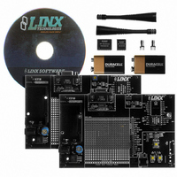
KIT MASTER DEV 869MHZ ES RS232
Manufacturer
Linx Technologies Inc
Type
Transmitterr
Datasheet
1.MDEV-869-ES-RS232.pdf
(7 pages)
Specifications of MDEV-869-ES-RS232
Frequency
869MHz
Product
RF Development Tools
Maximum Frequency
869 MHz
Supply Voltage (max)
9 V
Lead Free Status / RoHS Status
Lead free / RoHS Compliant
For Use With/related Products
Linx OEM Module
Lead Free Status / Rohs Status
Lead free / RoHS Compliant


USING THE DATA SQUELCH CIRCUIT
USING THE ENCODER AND DECODER
Page 6
A data squelch circuit is provided on the receiver development board. This circuit
is used to add both hysteresis and squelching capabilities as detailed in the ES
Series Receiver Data Guide. Since the ES Series receiver output is not internally
squelched, its output will continually hash when no transmission is present. This
can cause interrupts and buffer overflows in external circuitry. A squelch circuit
helps to eliminate hashing by providing a qualification threshold for incoming
data based on signal strength. This circuit is not a substitute for robust protocol
since squelch can be broken by unintended interference.
To get a better idea of the circuit’s operation, clip an oscilloscope probe on both
RX DATA and SQ. DATA (Squelch Data). With the transmitter off, the SQ. DATA
line will be high (which means that the output is squelched) while RX DATA will
be switching randomly. Squelching is accomplished by comparing RSSI with a
voltage reference created by R17 (potentiometer), R18, and R21. When the
RSSI falls below the voltage set by this reference, the output of the comparator
(U6) will pull to ground. This will disable the data slicer created with the additional
comparator contained within U6. It may be helpful to refer to the schematic
contained later in this document in order to better understand the entire function
of this circuit.
The squelch circuit will be at its factory default setting until the user adjusts it.
Remember that setting a higher squelch threshold can have a severe impact on
range. The squelch level affects only the threshold of the data going to the RS-
232 serial port and the SQ DATA line on TS2.
To set squelch, verify that the transmitter is off and turn on the receiver. Place
an oscilloscope probe on the SQ DATA line, and adjust R17 until SQ DATA
remains high. Two resistors (R27 and R28) are used to connect the module to
the squelch circuit. These may be removed to disconnect the squelch circuit and
prevent it from slightly loading the AUDIO and AUDIO REF lines.
The MS Series encoder and decoder use a 24-bit address to provide uniqueness
to the transmission and to prevent unintended activation. The development
boards come with a default address. To create a new address, press and hold
the CREATE button on the transmitter board. The address is randomized for as
long as the button is held down. Once released, the MODE_IND LED begins
flashing to indicate that the encoder is ready to accept Control Permissions.
Press the Buzzer and/or Relay buttons to indicate to the encoder that they will
be used. Press the Create button again to exit Create Mode, or let the encoder
time out after 15 seconds.
On the decoder board, press the LEARN button and the MODE_IND LED begins
flashing to indicate that the decoder is ready to learn a new address. Press one
of the authorized buttons on the transmitter board to send a signal. Press the
LEARN button again to exit Learn Mode, or let the decoder time out after 17
seconds and the system is ready for use.
The encoder and decoder can operate on one of four different baud rates as set
by the Baud Rate Selector switches. A faster baud rate will give a faster
response time. Please see the encoder or decoder data guide for the correct
settings. If the switch is up then it is connected to Vcc, if it is down then it is
connected to GND.
HOST INTERFACE MODULE
The ES Master Development System features a
Host Interface socket, which allows the use of
two different PC interface modules. The first is a
USB interface module that uses a standard USB
cable (not included) to connect to a PC’s USB
port or a USB hub. The second type of module
is a RS-232 interface module that can be
connected to a standard serial COM port on a
PC using a straight-through 9-pin extension
cable (not included). The evaluation board is
considered a DCE device and as such is
designed to be connected using a straight-thru
serial extension cable. Do not use a null-modem
cable as the boards will not function.
To install, select the module to be used and then
line up the pins on the module with the headers
on the board. Verify that the pin one polarity
marks on the board and on the Host Interface
Module match. The USB jack or the D-sub
connector should face away from the board.
Press firmly on the module so that it slides fully
into the header.
The development system may be prepared for host
operation with the supplied Linx software by setting
the jumpers on the header as shown in the
adjacent figure. This routes the module's data lines
to the Host Interface Module. Despite being
electrically interfaced, appropriate protocol must be
employed to ensure reliable and error-free data
transfer since the ES Series modules do not
encode or packetize the data in any manner. It is
important to understand that the development
boards are transparent; that is, the user's software
is entirely responsible for controlling the timing and error correction aspects of
the link.
incoming data. When designing a protocol to transfer data across a wireless link,
it is very important to remember that interference is inevitable. The protocol must
support error detection and correction if it is to be successful. A correctly
designed protocol will provide optimum performance and throughput for product-
specific applications while taking into account the timing and data-rate
requirements of the module. For further information on protocol considerations
please refer to Application Note AN-00160.
If the designer needs to develop protocols using a physical implementation other
than an RS-232 or USB interface, the designer can build the custom interface
circuitry in the prototyping area and route the module's data signals from the
header to the prototyping area.
The evaluation boards have no provision to check or qualify the
Figure 5: Host Interface Modules
Figure 6: Jumper Configuration
RS232 Interface Module
USB Interface Module
TS1
TX
PDN ENC
TX PDN
PDN RS232
TX RS232
TX DATA
TX ENCODER
/CLK
/CLK SEL
LO V DET
NC
GND
SQ. DATA
NC
AUDIO REF
AUDIO
RSSI
RX DATA
RX DECODER
RX PDN
RX
TS2
Page 7
Related parts for MDEV-869-ES-RS232
Image
Part Number
Description
Manufacturer
Datasheet
Request
R

Part Number:
Description:
KIT MASTER DEV 869MHZ ES USB
Manufacturer:
Linx Technologies Inc
Datasheet:

Part Number:
Description:
HOLDER BATTERY 20MM COIN CR2032
Manufacturer:
Linx Technologies Inc
Datasheet:

Part Number:
Description:
CONN RPSMA BL CRJA-CPV 8.5" COAX
Manufacturer:
Linx Technologies Inc

Part Number:
Description:
CABLE RG174 RPSMA M/F 8.5"
Manufacturer:
Linx Technologies Inc

Part Number:
Description:
CABLE RG174 SMA M/F 8.5"
Manufacturer:
Linx Technologies Inc

Part Number:
Description:
CABLE RPSMA/SMA 8.5"
Manufacturer:
Linx Technologies Inc

Part Number:
Description:
CABLE MALE-NMALE 8' RG-58 RPSMA
Manufacturer:
Linx Technologies Inc

Part Number:
Description:
CABLE RPSMA/SMA 8.5"
Manufacturer:
Linx Technologies Inc

Part Number:
Description:
CABLE MALE-NMALE 8' RG-58 SMA
Manufacturer:
Linx Technologies Inc

Part Number:
Description:
CONN RP-SMA FML BLKHD REAR RG174
Manufacturer:
Linx Technologies Inc

Part Number:
Description:
MODULE USB LOW SPEED
Manufacturer:
Linx Technologies Inc
Datasheet:

Part Number:
Description:
IC TRANSCODER MT BI-DIR 20-SSOP
Manufacturer:
Linx Technologies Inc
Datasheet:

Part Number:
Description:
IC ENCODER LOW SECURITY 8DIP
Manufacturer:
Linx Technologies Inc
Datasheet:

Part Number:
Description:
IC DECODER MS SERIES 20-SSOP
Manufacturer:
Linx Technologies Inc
Datasheet:
Part Number:
Description:
IC ENCODER MS SERIES 20-SSOP
Manufacturer:
Linx Technologies Inc
Datasheet: